
Treatment method of a getter material and encapsulation method of such getter material

a technology of encapsulation method and getter material, which is applied in the field of getter materials, can solve the problems of affecting the operation of the device,

Active Publication Date: 2011-04-07
COMMISSARIAT A LENERGIE ATOMIQUE ET AUX ENERGIES ALTERNATIVES
View PDF4 Cites 39 Cited by
  • Summary
  • Abstract
  • Description
  • Claims
  • Application Information

AI Technical Summary

Benefits of technology

[0007]Thus there is a need to propose a method for effectively protecting a getter material, for example intended to be encapsulated in a cavity in which a microelectronic and/or nanoelectronic device may also be enc

Problems solved by technology

The drawback to getter made in a thin layer is having strong reactivity with ambient air.
The presence of hydrogen in the getter material poses a problem since this hydrogen is released by getter material via desorption phenomenon when subjected to a temperature close to its activation temperature and under secondary vacuum, that is, at pressure between approximately 10−3 mbar and 10−7 mbar, these conditions frequently arising during encapsulation of the device and / or during thermal activation of the getter material.
But such degassing of hydrogen appearing after closing of the cavity encapsulating the device can be damaging to the operation of the device.
Also, formation of the oxide in the getter material by exposure to ambient air is poorly controlled since it depends inter alia on the partial pressure of water vapour in the ambient atmosphere which is random.
But such degassing can be obtained only by thermal treatment of the getter material over several hours, which represents a disadvantage for completing the encapsulation method.
This solution requires both making an additional deposit which, in addition to the extra costs generated, needs substantial control over the thickness of the protective layer of the noble metal, and also can add difficulties for forming the getter by photolithography and etching, or even may pose compatibility problems with technological stacking undertaken to construct the encapsulated micro-device.

Method used


Image

  • Treatment method of a getter material and encapsulation method of such getter material
  • Treatment method of a getter material and encapsulation method of such getter material
  • Treatment method of a getter material and encapsulation method of such getter material

Examples


Embodiment Construction

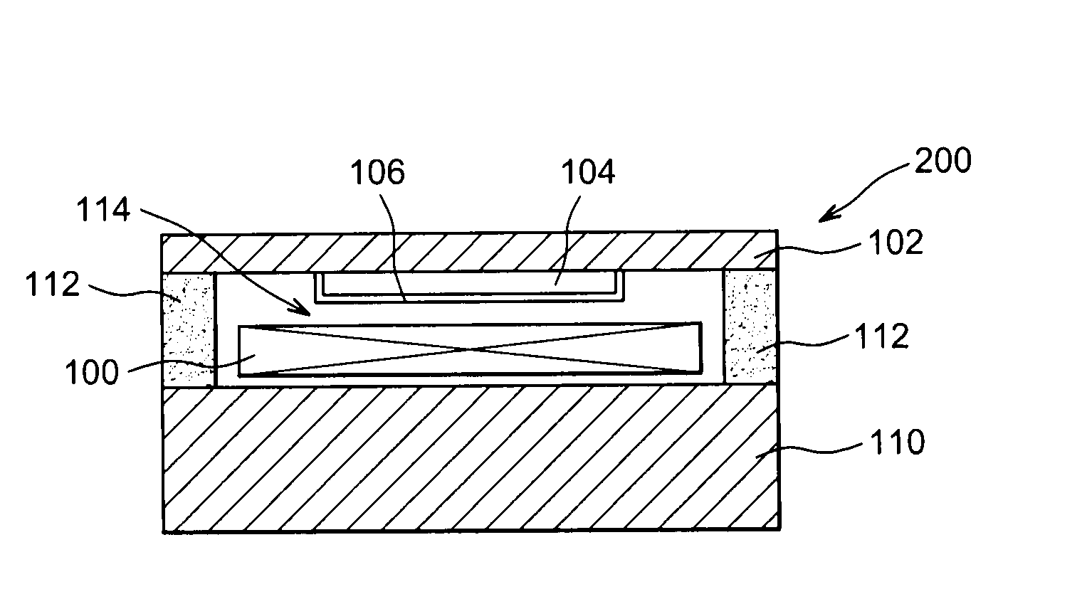
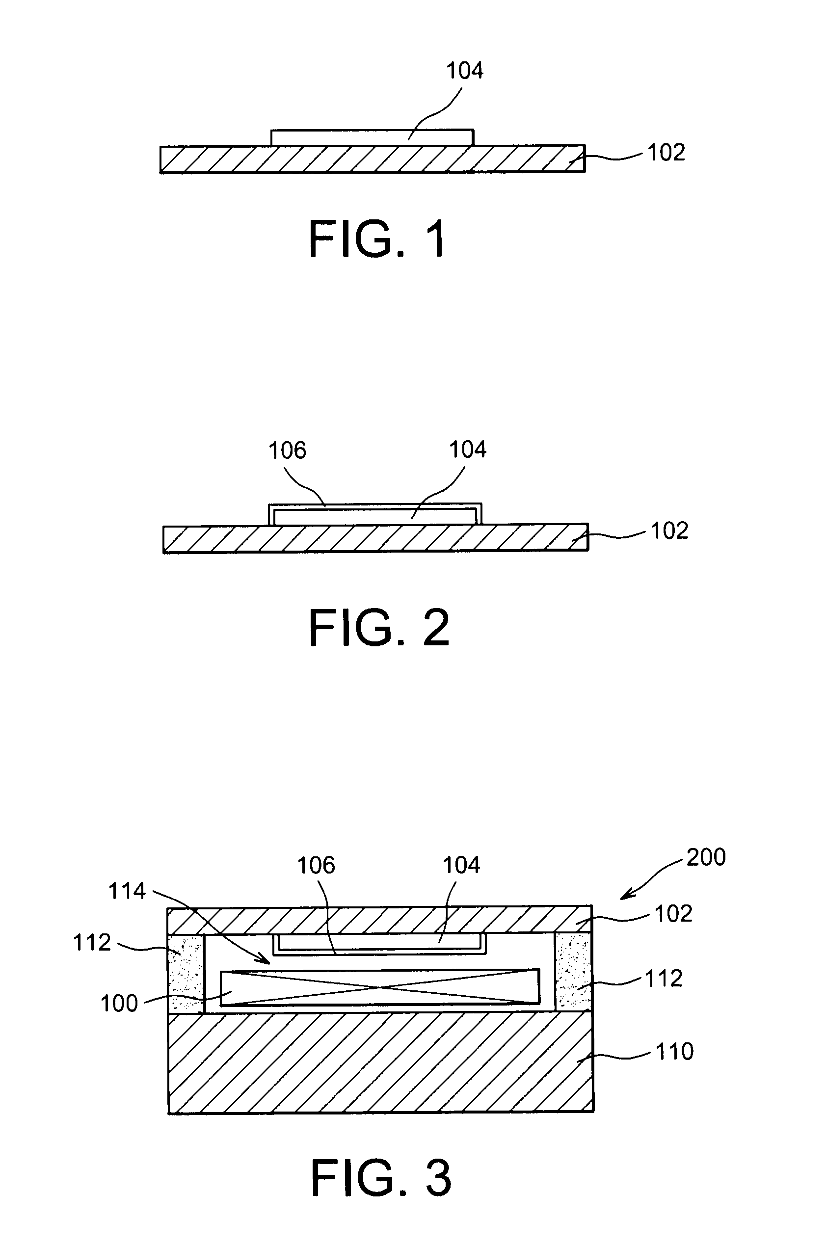
[0042]Reference is made to FIGS. 1 to 3 which illustrate the steps of an encapsulation method of a getter material 104 and of a microelectronic and / or nanoelectronic device 100, for example of MEMS and / or NEMS and / or MOEMS and / or NOEMS type, according to a particular embodiment.

[0043]As shown in FIG. 1, the getter material 104 is deposited on a substrate 102 intended to form the cover of a cavity in which the getter material 104 and the device 100 are intended to be encapsulated. The getter material 104, here titanium, is for example made by lift-off deposit (deposit through a sacrificial mask made on the substrate 102) or by deposit through a stencil, in the form of a thin layer, that is, whereof the thickness is less than or equal to approximately 10 μm. The getter material 104 may also be formed by lithography and etching.

[0044]Treatment of the getter material 104 is then carried out so that it is protected especially from ambient air. For this, dry dioxygen (O2) and / or dry dinit...


PUM

PropertyMeasurementUnit
Grain sizeaaaaaaaaaa
Temperatureaaaaaaaaaa

Abstract

A treatment method for a getter material, comprising at least one oxidation and / or nitriding step of getter material conducted under dry atmosphere of dioxygen and / or dinitrogen at pressure greater than approximately 10−2 mbar and at a temperature between approximately 50° C. and 120° C. and over a period between approximately 1 minute and 10 minutes, forming a protective layer composed of oxide and / or nitride of getter material.

Description

TECHNICAL FIELD[0001]The invention relates to the field of getter materials used to produce gaseous absorption and / or adsorption, for example in a closed cavity encapsulating a microelectronic and / or nanoelectronic device. The invention relates more particularly to carrying out protective treatment of such getter materials.PRIOR ART[0002]When encapsulation of a microelectronic and / or nanoelectronic device for example of MEMS (electromechanical microsystem) and / or NEMS (electromechanical nanosystem) and / or MOEMS (opto-electromechanical microsystem) and / or NOEMS (opto-electromechanical nanosystem) type is carried out in a hermetically sealed cavity, it is known to deposit a getter material in a thin layer inside the cavity, either to the side of the device or against the cover of the cavity, as described in documents U.S. Pat. No. 6,897,551 B2 and WO 2009 / 087284 A1. Getter material is a material comprising, intrinsically and / or via its microscopic or nanoscopic morphology, absorbent a...

Claims


Application Information

Patent Timeline
IPC IPC(8): H05K5/00H01J7/18B05D5/12
CPCB81C1/00285H01J29/94H01J2211/52H01L23/10H01L2924/0002H01L23/26H01L2924/00H01L2924/16195
Inventor BAILLIN, XAVIERLAGOUTTE, EMMANUELLERODRIGUEZ, GUILLAUME
Owner COMMISSARIAT A LENERGIE ATOMIQUE ET AUX ENERGIES ALTERNATIVES
Learn More