

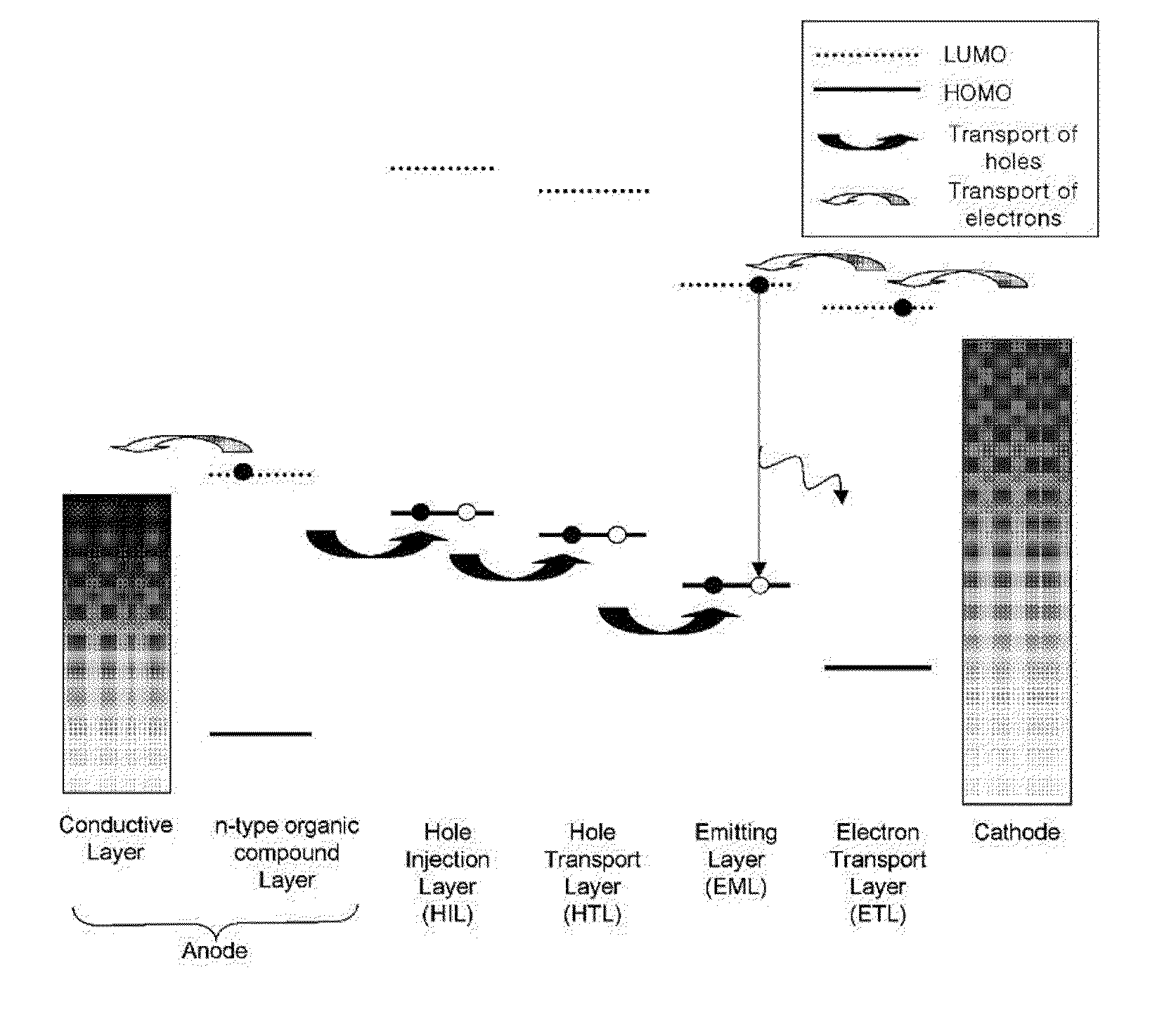
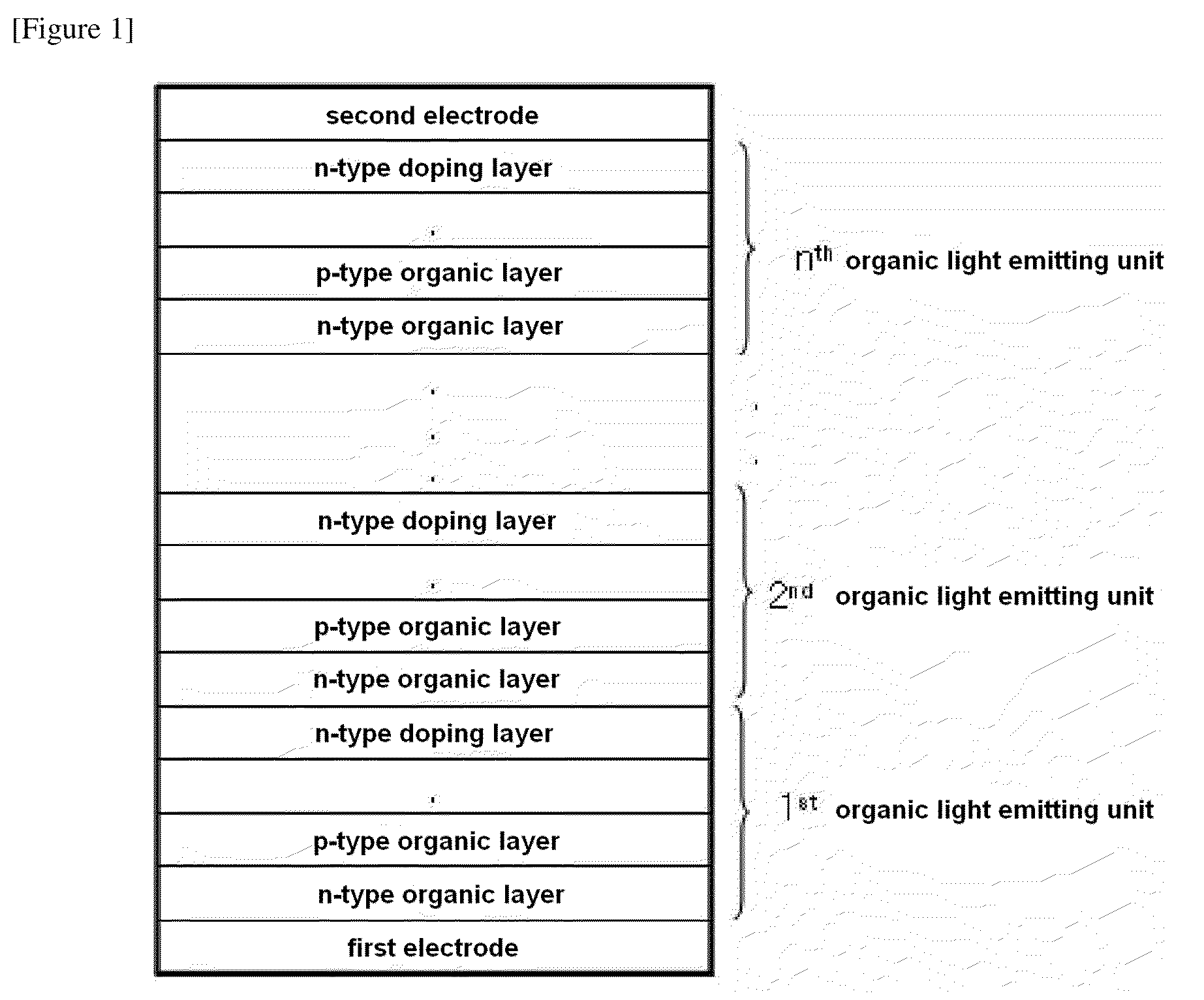
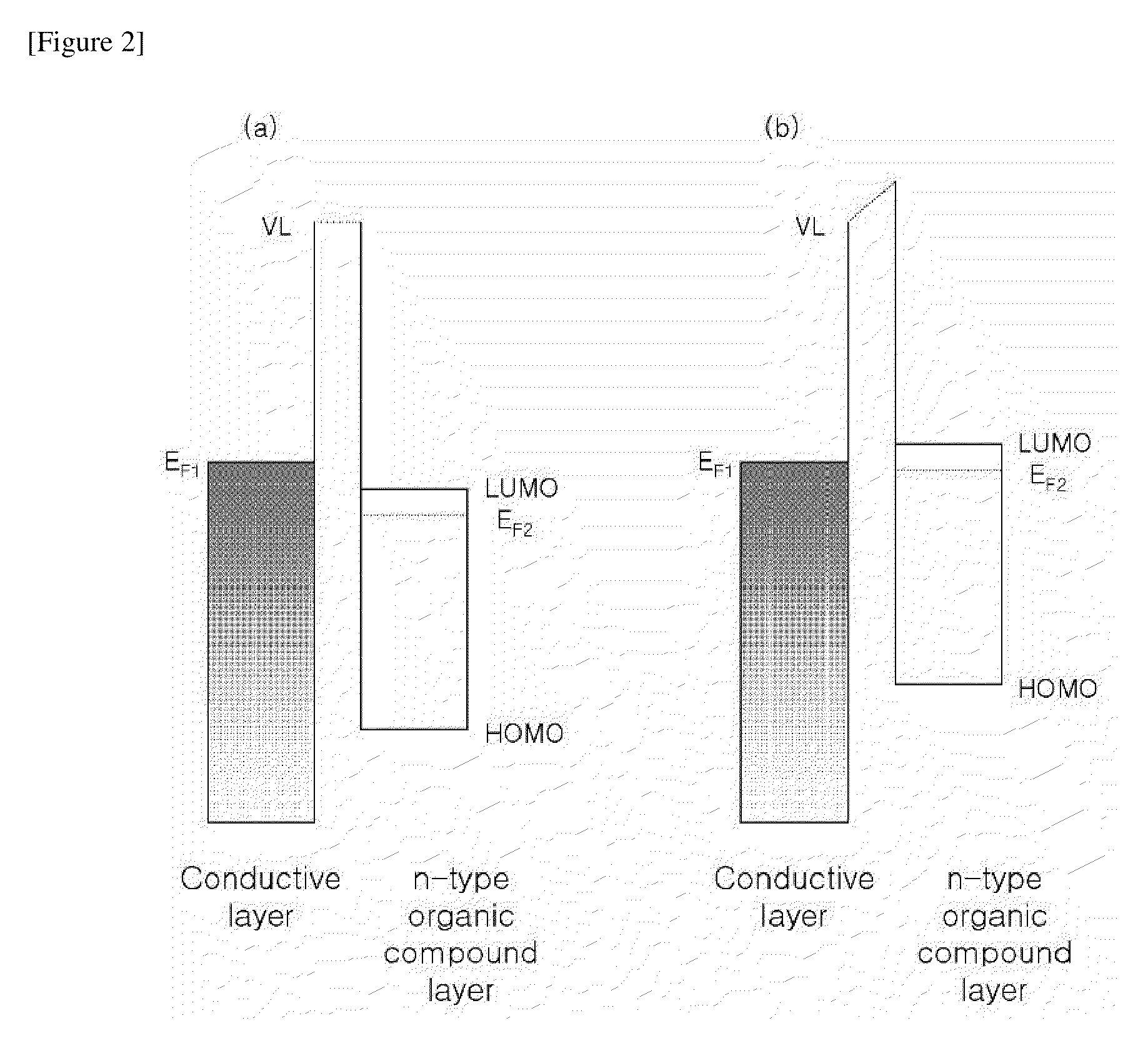
Stacked organic light emitting diode
a light-emitting diode and organic technology, applied in the direction of organic semiconductor devices, thermoelectric devices, luminescent compositions, etc., can solve the problems of limiting the selection of materials for the hole injection layer, negatively affecting the performance of the device, unstable interface between the electrode formed of metal, metal oxides or conductive polymers and the organic layer, etc., to achieve high brightness, simplify the process of manufacturing a device, and high brightness
- Summary
- Abstract
- Description
- Claims
- Application Information
AI Technical Summary
Benefits of technology
Problems solved by technology
Method used
Image

Examples
example 2
[0137]On the substrate, as IZO, the transparent anode (first electrode) that had the thickness of 1000 Å was formed by using the sputtering method, and HAT was vacuum deposited by heat thereon to form the n-type organic that had the thickness of 500 Å. NPB of the following Formula was vacuum deposited thereon to form the hole transport layer that had the thickness of 400 Å to form the NP conjunction.
[0138]In addition, Ir(ppy)3 of the following Formula was doped on CBP of the following Formula in an amount of 10 wt %, and the light emitting layer that had the thickness of 300 Å was constituted with the doped organic layer.
[0139]In addition, BAlq that was the hole interrupting layer material of the following Formula was formed in a thickness of 50 Å.
[0140]The electron transport layer material of the following Formula was formed in a thickness of 150 Å thereon. Ca was doped in an amount of 10 wt % to the electron transport material of the following Formula thereon, and the doped electr...
example 3
[0143]The stacked organic light emitting diode was manufactured by using the same method as the method of Example 3, except that 10 vol % of Mg was used instead of Ca as the n-type doped electron transport layer. This stacked diode structure is IZO / NPB / CBP+Ir(ppy)3 / BAlq / ETL / Mg+ETL / HAT / NPB / CBP+Ir(ppy)3 / BAlq / ETL / Mg+ETL / Al.
PUM
 Abstract
Description
Claims
Application Information