Method for testing through-silicon-via and the circuit thereof

a technology of throughsiliconvia and test circuit, which is applied in the direction of semiconductor/solid-state device testing/measurement, semiconductor/solid-state device details, instruments, etc., can solve the problems of 3d ic technology, compound yield loss due to ic stacking, and limitations of these test schemes

Active Publication Date: 2011-04-07
NATIONAL TSING HUA UNIVERSITY
View PDF11 Cites 69 Cited by
  • Summary
  • Abstract
  • Description
  • Claims
  • Application Information

AI Technical Summary

Problems solved by technology

In spite of the advantages mentioned above, there are some problems associated with 3D IC technology.
One of the most important issues is the compound yield loss due to IC stacking.
However, there are some limitations in these test schemes.
First, they cannot be performed before bonding.
Apparently, this scheme is suitable only for the wafer acceptance test (WAT), since it is extremely difficult, if not impossible, to dismantle and rework the back metal once the TSV test is done.
As a result, the observation of TSV failures at this stage relies solely on a couple of test keys on the scribe line.
Second, individual TSVs are indistinguishable in a serial scan chain or a daisy chain, so diagnosis becomes an issue.
Probing both ends of a TSV can measure its resistance as the pass / fail criterion, but the area overhead for direct access is high, and thus is limited to a small number of sparse TSVs.
However, there are not always flip-flops connected to both ends of each TSV.
In addition, the TSV failure rate affects the final yield exponentially with the number of dies in a stack.
Unfortunately, it remains relatively high (>10 ppm).
Without screening out the bad ones, the overall yield of the die stack will be low.

Method used


Image

  • Method for testing through-silicon-via and the circuit thereof
  • Method for testing through-silicon-via and the circuit thereof
  • Method for testing through-silicon-via and the circuit thereof

Examples


Embodiment Construction

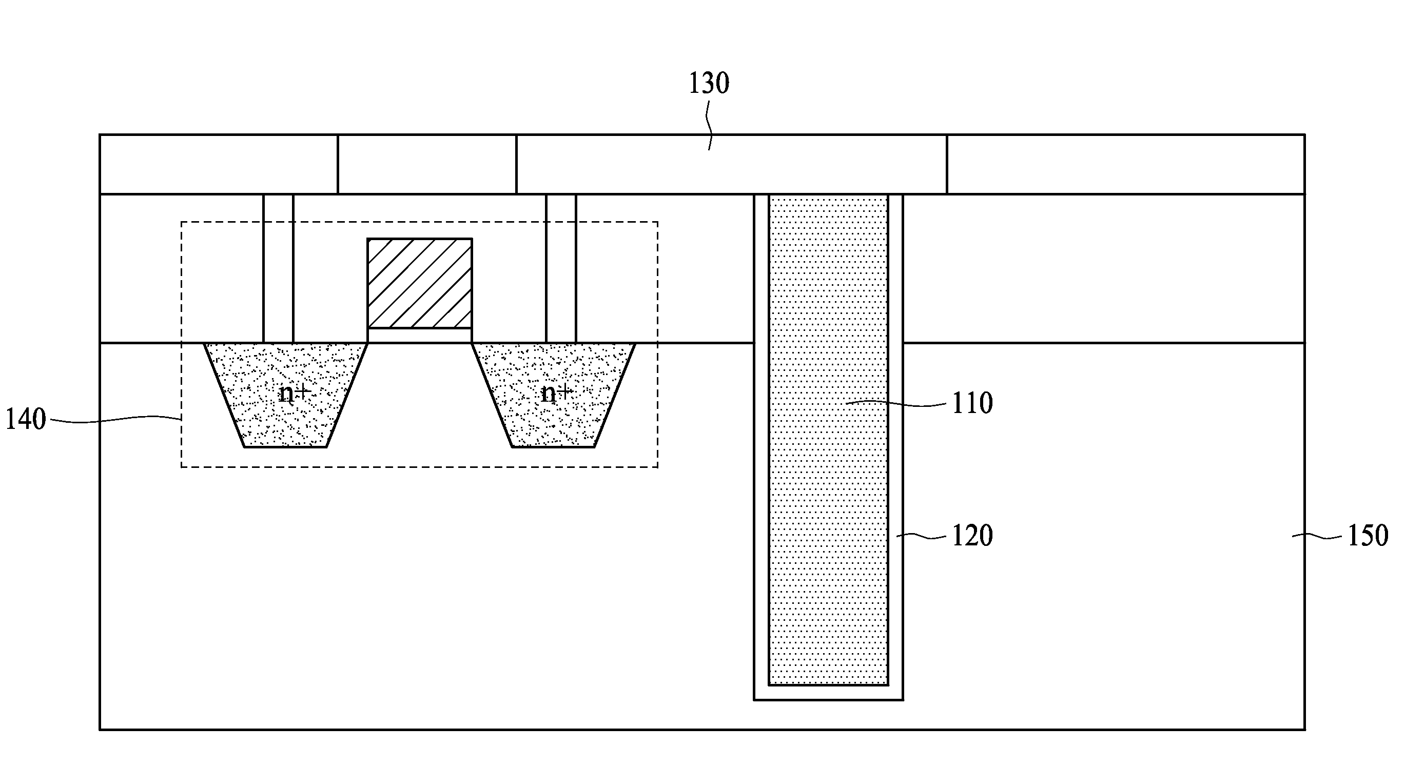
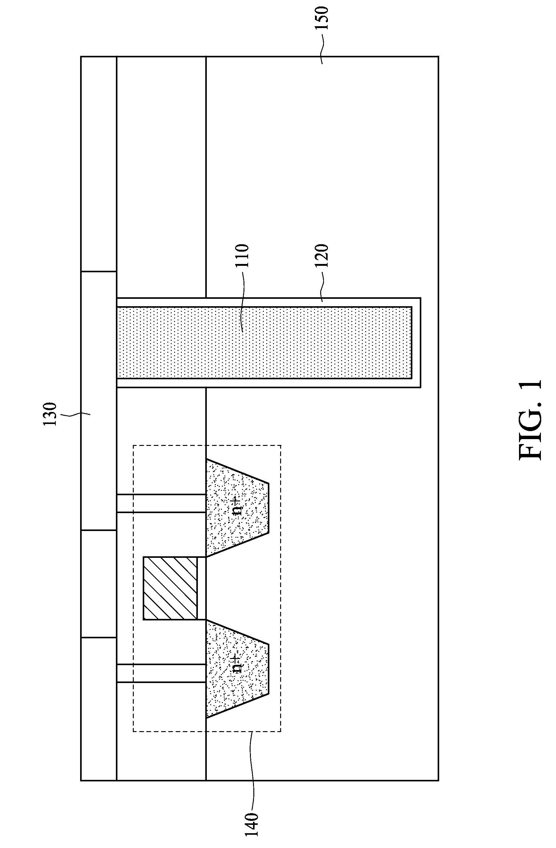
[0032]FIG. 1 shows a cross-section view of a TSV before wafer grinding / thinning on the backend. As shown in FIG. 1, the TSV 110 is formed in a substrate 150 and is electrically connected to an NMOS transistor 140 nearby. One end of the TSV 110 is connected to a metal layer 130, and the other end of the TSV 110 is floating with a surrounding dielectric layer 120 to insulate the TSV 110 from the substrate 150. It can be derived from FIG. 1 that since the TSV 110 is surrounded by the dielectric layer 120 within the substrate 150, the TSV 110 may exhibit a resistance property, a capacitance property or the combined property. It should be noted that a TSV cannot only applied to an NMOS transistor, it can be applied to a PMOS transistor or other active or passive components as well.

[0033]One type of defect of a TSV is a break type defect. A break in the TSV may cause an open failure. With such a failure, the signal does not pass from one end of the TSV to the other end in a specific perio...


PUM


Abstract

The method and circuit for testing a TSV of the present invention exploit the electronic property of the TSV under test. The TSV under test is first reset to a first state, and is then sensed at only one end to determine whether the TSV under test follows the behavior of a normal TSV, wherein the reset and sense steps are performed at only one end of the TSV under test. If the TSV under test does not follow the behavior of a normal TSV, the TSV under test is determined faulty.

Description

CROSS-REFERENCE TO A RELATED APPLICATION[0001]This application is a Continuation-In-Part (CIP) Application of U.S. patent application Ser. No. 12 / 572,030 filed on Oct. 1, 2009, the disclosure of which is incorporate herein by reference.BACKGROUND OF THE INVENTION[0002]1. Field of the Invention[0003]The present invention relates to a test method and a test circuit, and more particularly, to a method for testing a through-silicon-via and the circuit thereof.[0004]2. Description of the Related Art[0005]Three-dimensional integrated circuit (3D IC) technology, a promising technology in the field of modern electronics, is a technology in which two or more layers of active electronic components are integrated into a chip. In other words, a 3D IC packages a plurality of ICs into a single chip. Compared with a traditional single IC chip, a 3D IC provides a faster signal transmission rate between ICs, generates less noise, consumes less power, occupies less space and produces better performan...

Claims


Application Information

Patent Timeline
Patent Type & Authority Applications(United States)
IPC IPC(8): G01R31/26H01L23/522
CPCG01R31/2853H01L21/76898H01L22/14H01L22/34H01L2924/0002G01R31/2601H01L2924/00
Inventor WU, CHENG WENCHEN, PO YUANKWAI, DING MINGCHOU, YUNG FA
Owner NATIONAL TSING HUA UNIVERSITY
Why Eureka
Try Eureka