
Pellicle

a lithography and pellicle technology, applied in the field of lithography, can solve the problems of mask deformation, mask flatness can sometimes be degraded, defocusing within the exposure device, etc., and achieve the effect of suppressing the deformation of the exposure master pla

Inactive Publication Date: 2011-04-07
SHIN ETSU CHEM IND CO LTD
View PDF7 Cites 4 Cited by
  • Summary
  • Abstract
  • Description
  • Claims
  • Application Information

AI Technical Summary

Benefits of technology

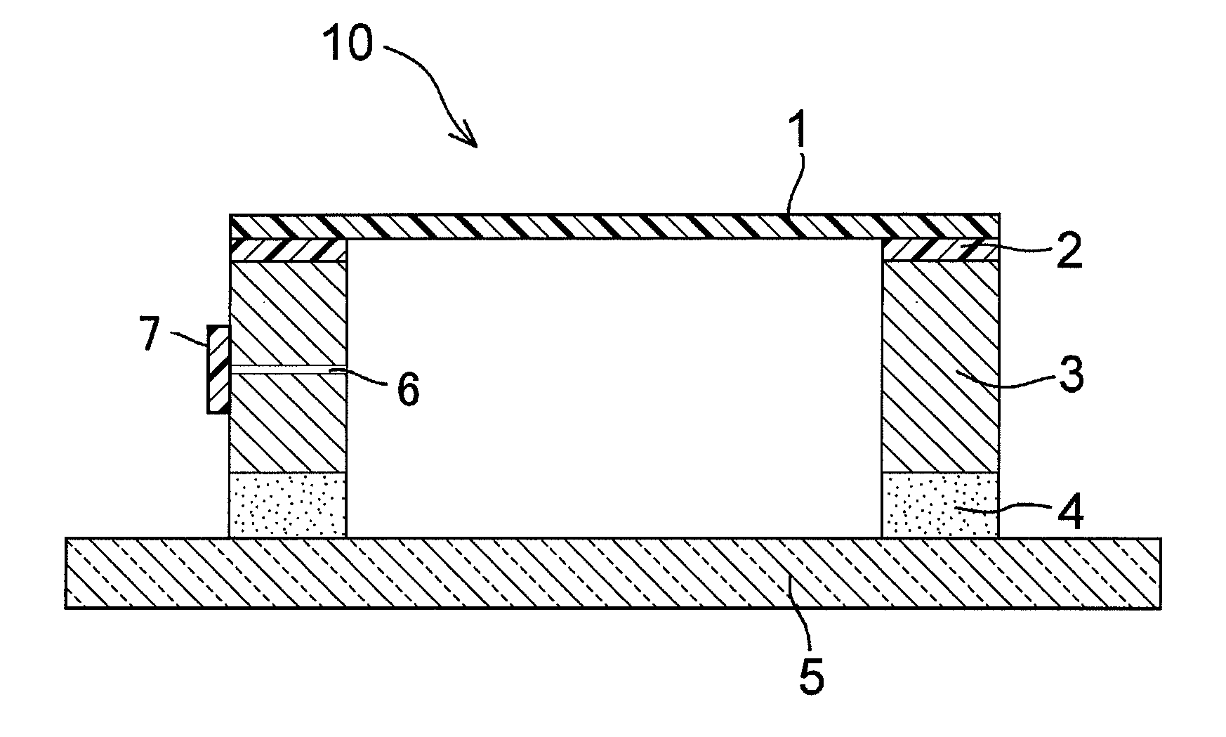
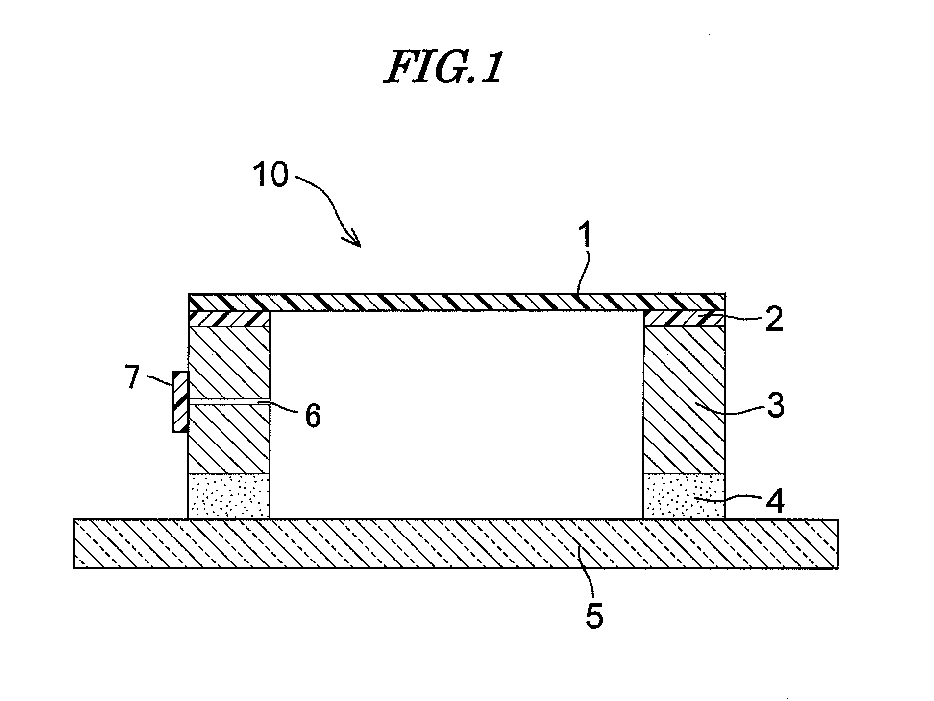
The present invention provides a pellicle for lithography that can prevent deformation of the mask when affixed. The pellicle comprises a pellicle frame, a pellicle film stretched over one end face of the pellicle frame, and a pressure-sensitive adhesion layer provided on the other end face. The pressure-sensitive adhesion layer comprises a gel composition with a specific consistency and thickness. The use of this pellicle can prevent distortion of the pattern image and improve the flatness of the mask, thus ensuring better exposure quality.

Problems solved by technology

In general, the flatness of a pellicle frame is in the order of 20 to 80 μm, but if a pellicle employing a pellicle frame having poorer flatness than the mask is affixed to the mask, the shape of the frame is transferred to the mask, thus causing deformation in the mask.
When the mask is deformed, the mask flatness can sometimes be degraded, and in this case the problem of defocusing within an exposure device occurs.
On the other hand, deformation of the mask can sometimes improve the flatness, but even in this case a pattern formed on the mask surface is distorted, and as a result the problem that a pattern image replicated on a wafer by exposure being distorted occurs.
Since this distortion of the pattern also occurs when the mask flatness is degraded, when the mask ends up being deformed by affixing the pellicle, the problem of the pattern image being distorted always occurs.

Method used


Image

  • Pellicle
  • Pellicle

Examples


example 1

[0040]An aluminum alloy pellicle frame (external dimensions 149 mm×113 mm×4.5 mm, thickness 2 mm, flatness on the pressure-sensitive adhesive layer side 30 μm) was washed with pure water, an end face thereof was coated with a silicone polymer gel (product name: KE-1051J) manufactured by Shin-Etsu Chemical Co., Ltd., and cured, thus forming a pressure-sensitive adhesion layer. Specifically, liquid A and liquid B of KE-1051J were mixed at a mixing ratio of 1:1 and placed in a syringe, coating was carried out using a dispenser, and subsequently curing was carried out at a curing temperature of 150° C. for a curing time of 10 min. The cured KE-1051J had a ¼ cone penetration in accordance with ASTM D-1403 of 65. The thickness of the cured KE-1051J was 0.3 mm.

[0041]Subsequently, the face of the pellicle frame opposite to the pressure-adhesive face was coated with a Cytop adhesive (product name: CTX-A) manufactured by Asahi Glass. Following this, the pellicle frame was heated at 130° C., t...

example 2

[0044]Pellicle 2 was completed in the same manner as in Example 1 except that the silicone polymer gel used in Example 1 was changed, and a silicone polymer gel (product name: X-32-1268) manufactured by Shin-Etsu Chemical Co., Ltd. was used.

[0045]The mixing ratio of liquid A and liquid B of X-32-1268 was 1:1, and curing conditions were a curing time of 10 min and a curing temperature of 150° C. The cured X-32-1268 had a ¼ cone penetration in accordance with ASTM D-1403 of 95. The thickness of the cured X-32-1268 was 0.3 mm.

[0046]When this pellicle 2 was affixed to a mask having a flatness of 0.20 μm, the flatness of the mask did not change and remained at 0.20 μm, this being very good result. The results thus obtained are shown in Table 1.

example 3

[0047]Pellicle 3 was completed in the same manner as in Examples 1 and 2 except that, unlike Examples 1 and 2, a urethane polymer gel (product name: Pandex GCA-11 / GCB-41) manufactured by DIC was used instead of the silicone polymer gel.

[0048]The mixing ratio of Pandex GCA-11 / GCB-41 was 100:12.5, and curing conditions were a curing time of 30 min and a curing temperature of 100° C. The cured Pandex GCA-11 / GCB-41 had a ¼ cone penetration in accordance with ASTM D-1403 of 55. The thickness of the cured Pandex GCA-11 / GCB-41 was 0.5 mm.

[0049]When this pellicle 3 was affixed to a mask having a flatness of 0.20 μm, the flatness of the mask changed to 0.22 μm. The amount of change in the flatness of the mask after affixing the pellicle was a low value of 0.02 μm, this being a good result. The results thus obtained are shown in Table 1.


PUM

PropertyMeasurementUnit
thicknessaaaaaaaaaa
thicknessaaaaaaaaaa
thicknessaaaaaaaaaa

Abstract

A pellicle for lithography is provided that includes a pellicle frame, a pellicle film stretched over one end face of the pellicle frame, and a pressure-sensitive adhesion layer provided on the other end face, the pressure-sensitive adhesion layer being formed from a gel composition.

Description

BACKGROUND OF THE INVENTION[0001]1. Field of the Invention[0002]The present invention relates to a pellicle for lithography used as a debris shield for a lithography mask when producing a semiconductor device such as an LSI or a ULSI or a liquid crystal display panel.[0003]2. Description of the Related Art[0004]In the production of a semiconductor such as an LSI or a ULSI or the production of a liquid crystal display panel, a pattern is formed by irradiating a semiconductor wafer or a liquid crystal master plate with light; if debris is attached to an exposure master plate, since the debris absorbs the light or refracts the light, there are problems that the replicated pattern is deformed, the edges become rough, or the background is stained black, thus impairing the dimensions, quality, appearance, etc. The ‘exposure master plate’ referred to in the present invention is a general term for lithography masks (also called simply ‘masks’) and reticles. The explanation below is given fo...

Claims


Application Information

Patent Timeline
Patent Type & Authority Applications(United States)
IPC IPC(8): G03F1/00G03F1/62
CPCG03F1/142G03F1/64G03F1/62H01L21/0274
Inventor SHIRASAKI, TORUTSUKADA, JUNICHI
Owner SHIN ETSU CHEM IND CO LTD
Learn More