Oxide semiconductor layer and semiconductor device

a semiconductor layer and oxide technology, applied in the field of semiconductor layers, can solve the problems of insufficient characteristics, and achieve the effects of excellent characteristics, excellent electric characteristics, and highly reliable oxide semiconductor layers

Active Publication Date: 2011-04-14
SEMICON ENERGY LAB CO LTD
View PDF99 Cites 89 Cited by
  • Summary
  • Abstract
  • Description
  • Claims
  • Application Information

AI Technical Summary

Benefits of technology

[0022]Electric characteristics of an oxide semiconductor layer which employs a crystal structure having electrical anisotropy in a vicinity of a surface is changed in comparison with those of an oxide semiconductor layer which does not employ the crystal structure. For example, conductivity in a direction parallel to the surface of the oxide semiconductor layer is improved, and an insulating property in a direction vertical to the surface of the oxide semiconductor layer is improved.
[0024]Therefore, according to one embodiment of the disclosed invention, an oxide semiconductor layer having excellent electric characteristics is provided. In addition, a highly reliable oxide semiconductor layer is provided.
[0025]According to another embodiment of the disclosed invention, a semiconductor device having excellent characteristics is provided. In addition, a highly reliable semiconductor device is provided.

Problems solved by technology

However, in the real condition, adequate characteristics have not been obtained even when such oxide semiconductors are used.

Method used


Image

  • Oxide semiconductor layer and semiconductor device
  • Oxide semiconductor layer and semiconductor device
  • Oxide semiconductor layer and semiconductor device

Examples


embodiment 1

[0051]In this embodiment, an oxide semiconductor layer according to one embodiment of the disclosed invention, a manufacturing method thereof, and the like will be described in detail with reference to FIGS. 1A and 1B, FIG. 2, FIGS. 3A to 3C, FIGS. 4A and 4B, FIGS. 5A-1 to 5A-6 and 5B, FIGS. 6A-1 to 6A-3 and 6B-1 to 6B-3, FIGS. 7A and 7B, FIGS. 8A-1, 8A-2, 8B-1, and 8B-2, FIG. 9, FIG. 10, FIGS. 11A to 11D, FIG. 12, FIG. 13, and FIGS. 14A to 14C.

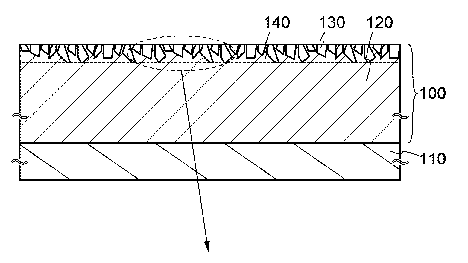
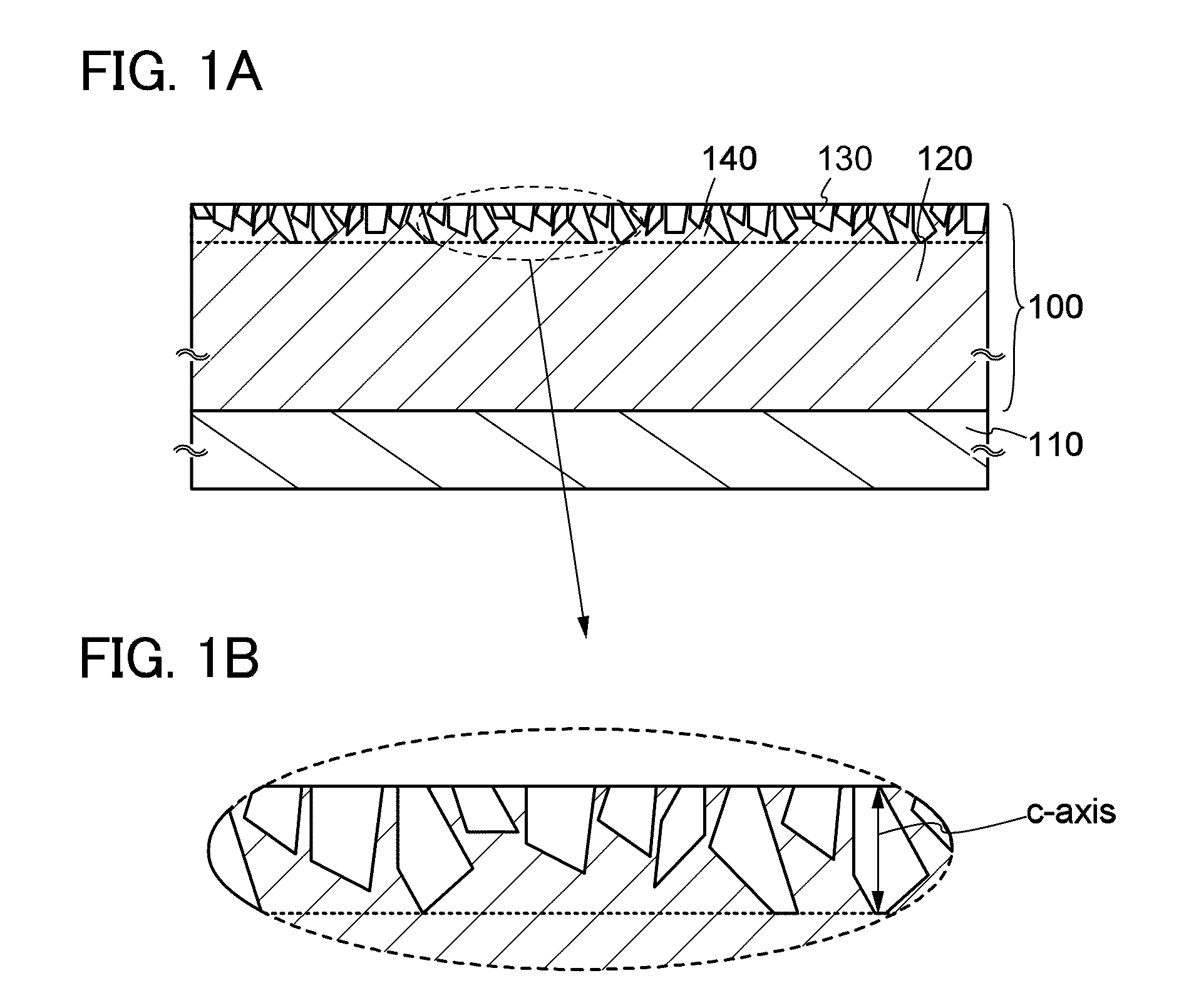
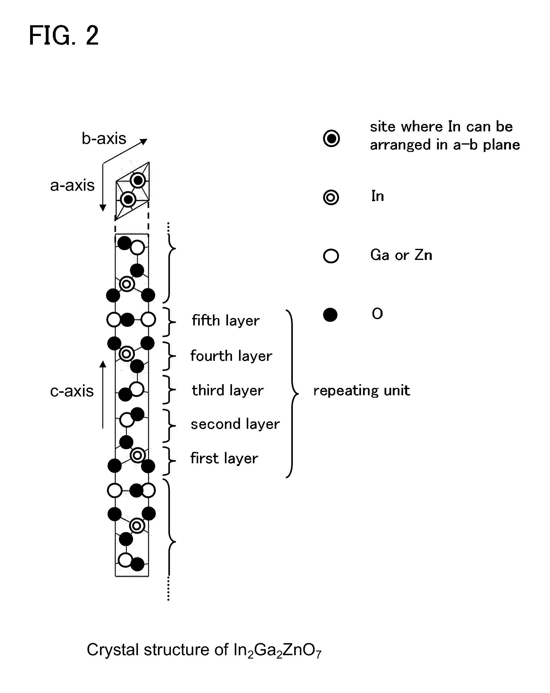
[0052]First, a structure of an oxide semiconductor layer is described with reference to FIGS. 1A and 1B and FIG. 2.

[0053]FIGS. 1A and 1B show an example where an oxide semiconductor layer 100 is provided on a surface on which a base material 110 is to be formed. Note that any material may be used for the base material 110 as long as it can support the oxide semiconductor layer 100. The oxide semiconductor layer 100 is not limited to being provided on the surface on which the base material 110 is to be formed and may be a self-supported layer....

embodiment 2

[0108]In this embodiment, an example of a transistor as a semiconductor device and a manufacturing method thereof will be described with reference to FIGS. 15A to 15D and FIGS. 16A to 16D.

[0109]First, a conductive layer 302 is formed over a substrate 300 (see FIG. 15A).

[0110]Any substrate can be used for the substrate 300 as long as it is a substrate having an insulating surface, for example, a glass substrate. It is preferable that the glass substrate be a non-alkali glass substrate. As a material of the non-alkali glass substrate, a glass material such as aluminosilicate glass, aluminoborosilicate glass, or barium borosilicate glass is used, for example. Besides, as the substrate 300, an insulating substrate formed using an insulator such as a ceramic substrate, a quartz substrate, or a sapphire substrate, a semiconductor substrate which is formed using a semiconductor material such as silicon and whose surface is covered with an insulating material, or a conductive substrate whic...

embodiment 3

[0134]In this embodiment, another example of a transistor as a semiconductor device and a manufacturing method thereof will be described with reference to FIGS. 17A to 17D and FIGS. 18A to 18D. Note that many parts of a method for manufacturing a semiconductor device in this embodiment are common to those in the above embodiments; therefore, description of the common parts is omitted below and only different parts will be described in detail.

[0135]First, a conductive layer 402 is formed over a substrate 400 (see FIG. 17A). The above embodiments (the description with reference to FIG. 4A and the like) can be referred to for the details of the substrate 400, the conductive layer 402, and the like. A base layer may be formed over the substrate 400. The above embodiment can also be referred to for the details of the base layer.

[0136]Next, a resist mask 404 is selectively formed over the conductive layer 402 and the conductive layer 402 is selectively etched using the resist mask 404, wh...


PUM


Abstract

An object is to provide an oxide semiconductor layer having a novel structure which is preferably used for a semiconductor device. Alternatively, another object is to provide a semiconductor device using an oxide semiconductor layer having the novel structure. An oxide semiconductor layer includes an amorphous region which is mainly amorphous and a crystal region containing crystal grains of In2Ga2ZnO7 in a vicinity of a surface, in which the crystal grains are oriented so that the c-axis is almost vertical with respect to the surface. Alternatively, a semiconductor device uses such an oxide semiconductor layer.

Description

TECHNICAL FIELD[0001]The technical field of the disclosed invention relates to a semiconductor layer including an oxide semiconductor. Alternatively, the technical field of the disclosed invention relates to a semiconductor device using the semiconductor layer.BACKGROUND ART[0002]A field-effect transistor is one of the most widely-used semiconductor elements. A variety of materials are used for field-effect transistors according to their uses. In particular, semiconductor materials including silicon are frequently used.[0003]The field-effect transistor using silicon has characteristics satisfying the needs with respect to a variety of uses. For example, single crystal silicon is used for an integrated circuit or the like which needs to be operated at a high speed, whereby the need with respect to the integrated circuit is satisfied. Further, amorphous silicon is used for an object which needs a large area, such as a display device, whereby the need with respect to the object can be ...

Claims


Application Information

Patent Timeline
Patent Type & Authority Applications(United States)
IPC IPC(8): H01L29/12
CPCH01L29/7869H01L29/78693H01L29/78606H01L29/78618H01L29/78696H01L21/324H01L29/04H01L29/045
Inventor YAMAZAKI, SHUNPEISAKAKURA, MASAYUKIMIYANAGA, AKIHARUTAKAHASHI, MASAHIROHIROHASHI, TAKUYASHIMAZU, TAKASHI
Owner SEMICON ENERGY LAB CO LTD
Why Eureka
Try Eureka