Unlock instant, AI-driven research and patent intelligence for your innovation.

MEMS device with a composite back plate electrode and method of making the same

Inactive Publication Date: 2011-04-14
UNITED MICROELECTRONICS CORP
View PDF7 Cites 2 Cited by
  • Summary
  • Abstract
  • Description
  • Claims
  • Application Information

AI Technical Summary

Benefits of technology

[0007]It is one objective of the present invention to provide a fabricating method to prevent undercut when forming a vent pattern in a MEMS microphone. The method of the present invention is compatible with the method for forming a semiconductor device.
[0010]The feature of the present invention is that the aforesaid interlayer material does not react with halogen radicals. Therefore, the interlayer material disposed on the substrate can serves as a protective layer of the substrate. In this way, the undercut formed during the traditional fabrication of the vent pattern can be prevented.

Problems solved by technology

However, an undercut is formed on the silicon substrate when the etchant for the vent pattern contacts the silicon oxide layer or other isolating layers.
The undercut will damage the integrity of the MEMS microphone, thereby causing the performance of the MEMS microphone to deteriorate.

Method used


Image

  • MEMS device with a composite back plate electrode and method of making the same
  • MEMS device with a composite back plate electrode and method of making the same
  • MEMS device with a composite back plate electrode and method of making the same

Examples


Embodiment Construction

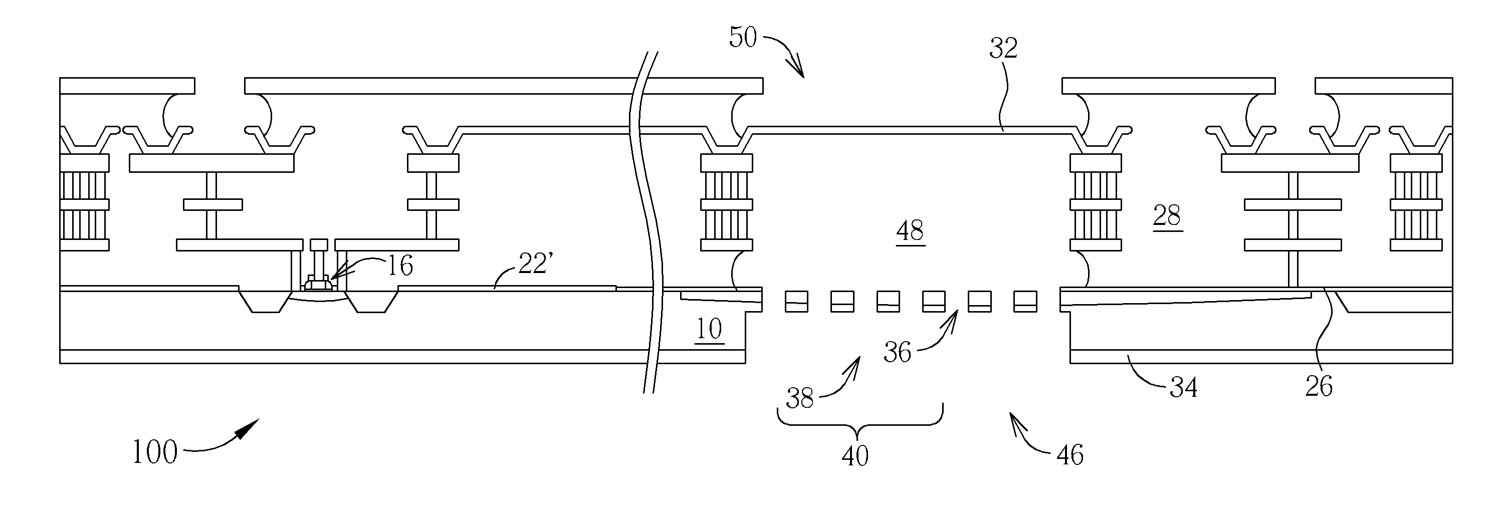
[0014]FIG. 1 to FIG. 13 are diagrams schematically depicting the method of fabricating a MEMS microphone. As shown in FIG. 1, first, a substrate 10 comprising a first surface 12 such as an active area and a second surface 14 such as a backside is provided. The substrate 10 includes at least one logic region A and at least one MEMS region B. A logic device 16 is disposed on the first surface 12 of the substrate 10 within the logic region A. The MEMS region B of the substrate 10 further includes a doped region 18 such as a P-type doped region or a N-type doped region. The logic device 16 may be a transistor such as a MOS transistor or a CMOS transistor. The substrate 10 may be a silicon on insulator (SOI) substrate, a single crystalline substrate or a multiple crystalline substrate. Then, a salicide block layer 20 such as silicon oxide, silicon or other dielectric materials is formed entirely on the first surface 12 of the substrate 10 within the MEMS region B and the logic region A. ...


PUM


Abstract

A method of fabricating MEMS device includes: providing a substrate with a first surface and a second surface. The substrate includes at least one logic region and at least one MEMS region. The logic region includes at least one logic device positioned on the first surface of the substrate. Then, an interlayer material is formed on the first surface of the substrate within the MEMS region. Finally, the second surface of the substrate within the MEMS region is patterned. After the pattern process, a vent pattern is formed in the second surface of the substrate within the MEMS region. The interlayer material does not react with halogen radicals. Therefore, during the formation of the vent pattern, the substrate is protected by the interlayer material and the substrate can be prevented from forming any undercut.

Description

BACKGROUND OF THE INVENTION[0001]1. Field of the Invention[0002]The present invention relates to a MEMS device and the fabricating method of the MEMS device, and more particularly, to a MEMS microphone and a fabricating method of the MEMS microphone.[0003]2. Description of the Prior Art[0004]The demand for MEMS devices such as MEMS microphones and MEMS speakers is increasing. Many cell phones are equipped with MEMS speakers for broadcasting ring tones and MEMS microphones for video recording. These MEMS microphones and MEMS speakers can also be applied to other portable digital devices with flash memories.[0005]MEMS microphones work on a principle of variable capacitance and voltage by the movement of an electrically charged diaphragm relative to a backplate electrode in response to sound pressure. The backplate electrode has a vent pattern with a plurality of trenches, wherein the vent pattern is usually formed by an etching process. However, an undercut is formed on the silicon su...

Claims


Application Information

Patent Timeline
IPC IPC(8): H01L29/84H01L21/30
CPCB81B2201/0257B81B2207/015B81C2203/0735B81C2201/014B81C1/00801
Inventor HUANG, CHIEN-HSINLAN, BANG-CHIANGWANG, MING-IWU, HUI-MINSU, TZUNG-ISU, CHAO-ANTAN, TZUNG-HANCHEN, MINLIN, MENG-JIA
Owner UNITED MICROELECTRONICS CORP