Method of depositing metallic film and memory medium

Active Publication Date: 2011-04-14
TOKYO ELECTRON LTD
View PDF2 Cites 7 Cited by
  • Summary
  • Abstract
  • Description
  • Claims
  • Application Information

AI Technical Summary

Benefits of technology

[0012]According to the present invention, a process for performing the deposition of the metallic film for plural pieces of substrates to be processed includes a step of forming the conductive film in the chamber one or more times. Thus, an abnormal discharge between the substrate and a stage may be suppressed because the formed conductive film makes the electrical charge in the substrate to flow into the stage even when the polymer gets accumulated on the stage area corresponding to the periphery portion of the substrate.

Problems solved by technology

Also, since the ashing process and the wet cleaning process are performed with a single wafer type, these processes may not be performed sufficiently for the back side of the wafer and the wafer is introduced into the Ti film forming chamber with the polymer residue at the back side of the wafer.
When the high frequency electric power is applied to generate plasma at this state, an abnormal discharge may occur at an area where the microgap is produced, and there is concern that troubles in products or damage in stage may occur.

Method used


Image

  • Method of depositing metallic film and memory medium
  • Method of depositing metallic film and memory medium
  • Method of depositing metallic film and memory medium

Examples


case 1

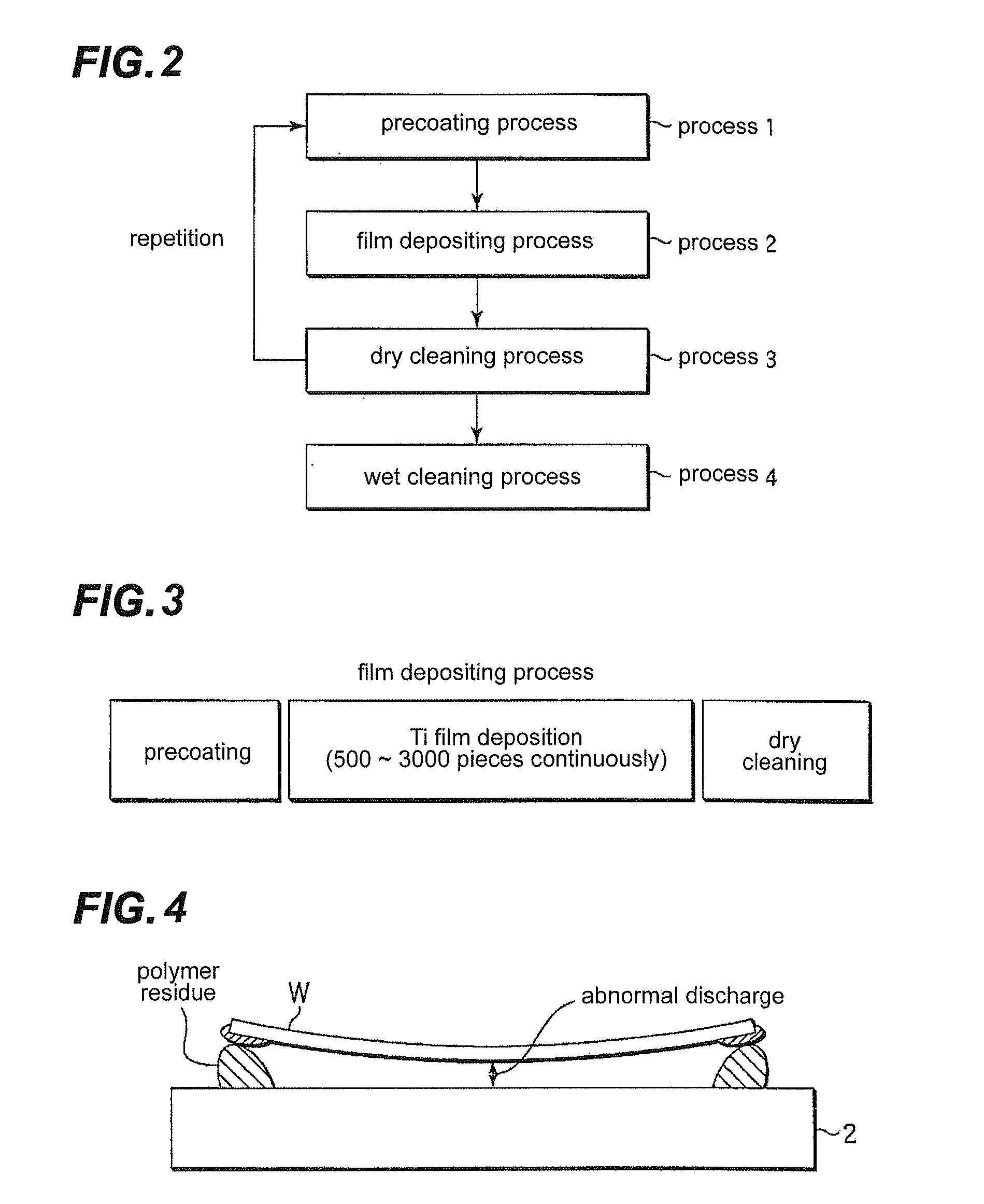
[0104]Case 1 shown in FIG. 9 is a conventional method performing a continuous film deposition process (Ti deposition+nitriding process) for 500 pieces of wafers W after the precoating, and then performing the dry cleaning process. As shown in FIG. 9, it is confirmed that the Vdc variation after 250 pieces of the wafers W is unstable, and the abnormal discharge may easily occur.

[0105]Therefore, in case 2 as shown in FIG. 10, the precoating process has been added after the Vdc variation occurred (after the film deposition of 254 pieces). And as a result, Vdc has been temporarily stabilized. That is, it is confirmed that performing the precoating process to form the conductive film on susceptor 2 in the course of repeating the film deposition process for a plurality of wafers W is effective for preventing the abnormal discharge. However, after the precoating process, Vdc becomes unstable again when the processed pieces of the wafers W are about 420 pieces, which proves that performing ...


PUM

PropertyMeasurementUnit
Electrical conductoraaaaaaaaaa
Metallic bondaaaaaaaaaa

Abstract

For depositing a metallic film, the following steps are repeatedly conducted: a step in which a precoat film is formed on the inside of a chamber; a step in which two or more substrates to be treated are subjected to the deposition of a metallic film thereon by introducing each substrate into the precoated chamber, placing the substrate on the stage, feeding a treating gas while heating the substrate to generate a plasma of the treating gas, and depositing a metallic film on the substrate by plasma CVD; and a step in which after the film deposition on the substrates has been completed, a cleaning gas is introduced into the chamber to conduct dry cleaning. In the step in which two or more substrates to be treated are subjected to the deposition of a metallic film thereon, a conductive film is formed on the stage one or more times in the course of the step.

Description

FIELD OF INVENTION[0001]The present invention relates to a method of depositing a metallic film by CVD in a chamber, and memory medium.BACKGROUND OF THE INVENTION[0002]In manufacturing semiconductor devices, owing to the recent demands of increased miniaturization and integration, circuit configuration is getting increasingly finer. Also, according to the requirement of forming a metallic film used for an interconnection layer, a burying layer, and a contact layer etc., with a favorable step coverage, CVD (Chemical Vapor Deposition) has been selected.[0003]For example, a single type plasma CVD is utilized in case of depositing Ti film with CVD to be used as a contact layer. In the single type plasma CVD, semiconductor wafers (hereinafter, wafers) each of which is a substrate to be processed is introduced into a chamber one piece at a time, and plasma is generated using, for example, TiCl4 gas as a source gas and H2 gas as a reduction gas, thereby forming Ti film on the wafer dispose...

Claims


Application Information

Patent Timeline
IPC IPC(8): C23C16/06C23C16/50
CPCC23C16/4405C23C16/50C23C16/4404H01L21/285
Inventor OKABE, SHINYA
Owner TOKYO ELECTRON LTD
Why Eureka
Try Eureka