Metal structure of flexible multi-layer substrate and manufacturing method thereof

Active Publication Date: 2011-04-21
PRINCO CORP
View PDF7 Cites 6 Cited by
  • Summary
  • Abstract
  • Description
  • Claims
  • Application Information

AI Technical Summary

Benefits of technology

[0025]Specifically, the metal structure of the multi-layer substrate according to the present invention can be flexible and not only applied in the field of package substrates. Meanwhile, the present invention also can be applied in the technical field of manufacturing print circuit boards and flexible package substrates. Significantly, the manufacturing method of the present invention attends to provide a metal structure

Problems solved by technology

Traditional flexible multi-layer substrates according to prior arts can only be manufactured with two or three layers.
A common problem which often occ

Method used


Image

  • Metal structure of flexible multi-layer substrate and manufacturing method thereof
  • Metal structure of flexible multi-layer substrate and manufacturing method thereof
  • Metal structure of flexible multi-layer substrate and manufacturing method thereof

Examples


first embodiment

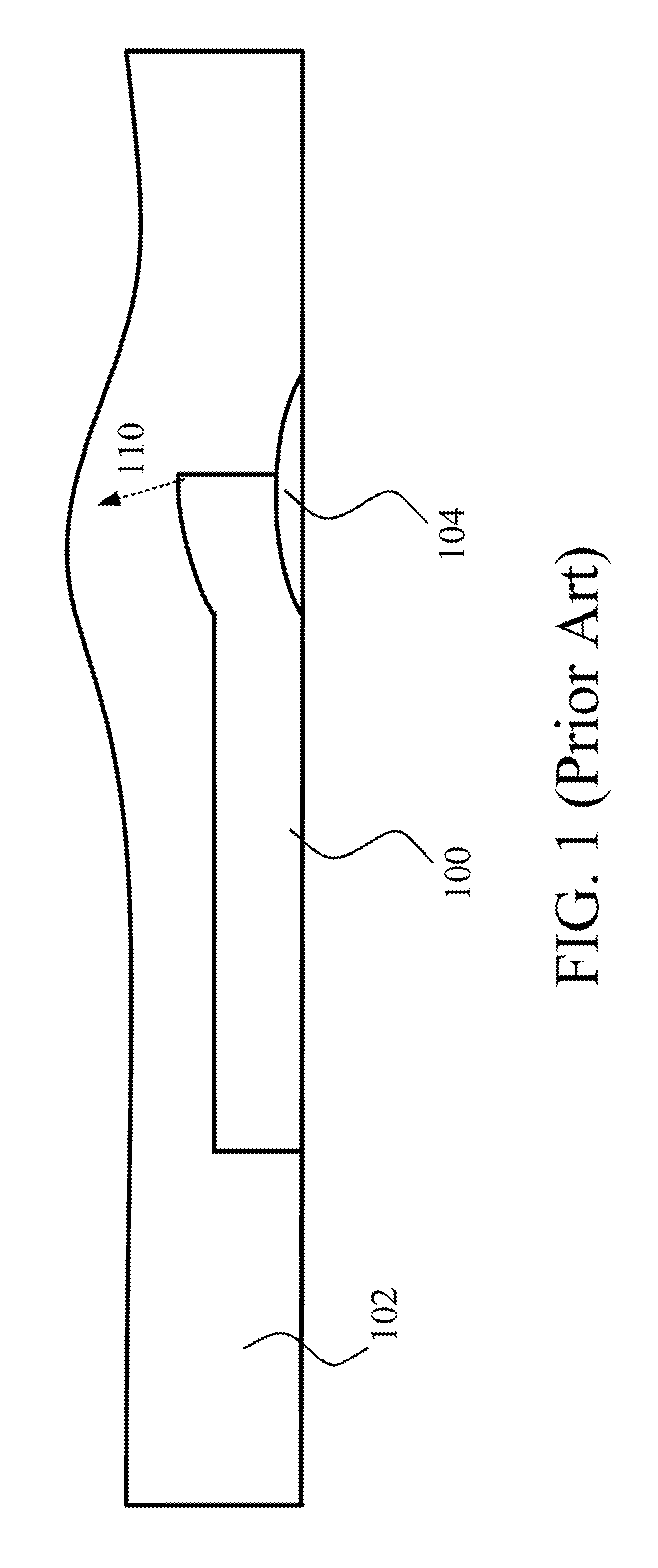
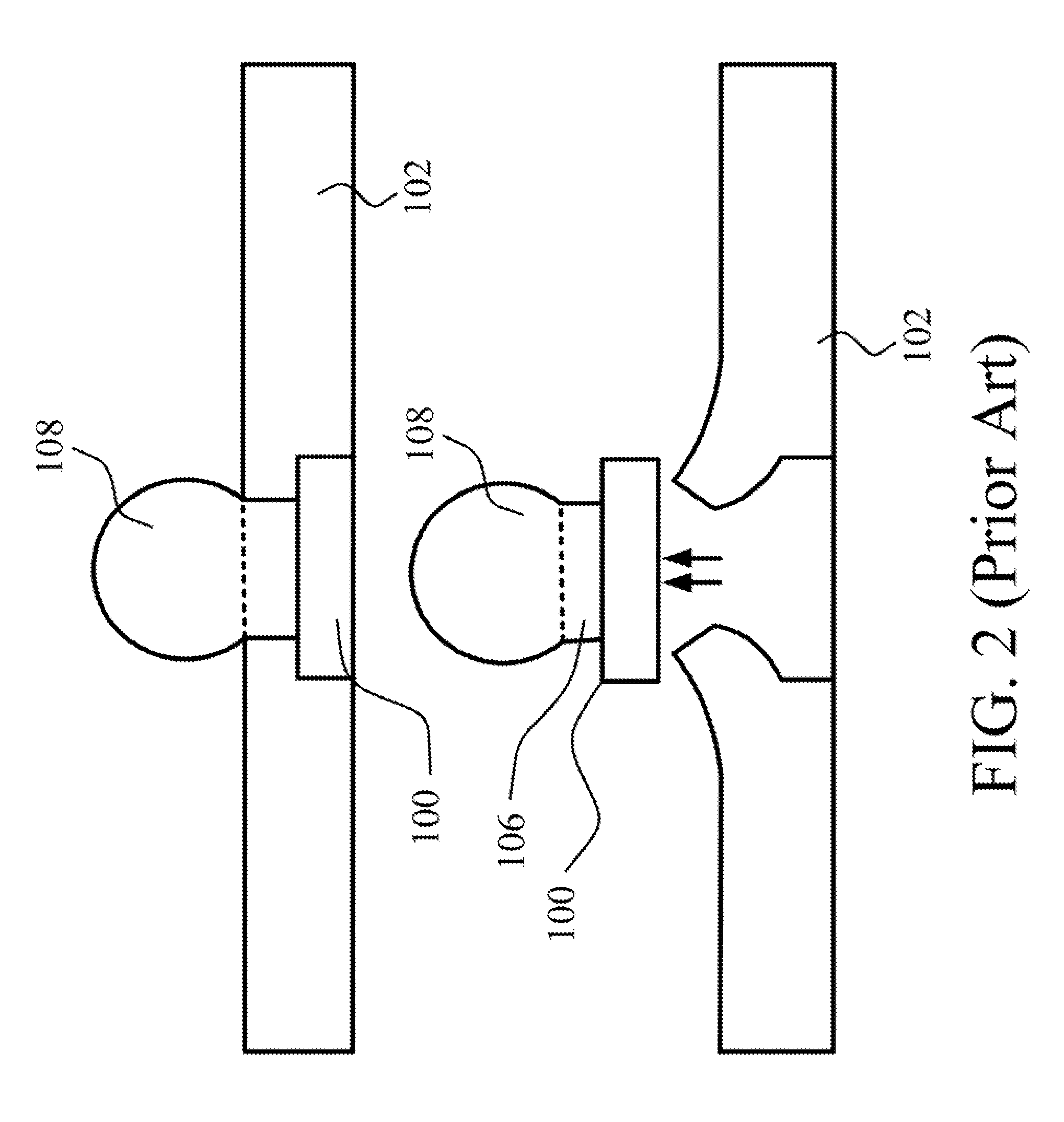
[0037]Please refer to FIG. 5, which depicts a diagram for explaining a manufacturing method for the metal structure of the multi-layer substrate according to the present invention. Please also refer to FIG. 3 at the same time. The manufacturing method of the metal structure of the flexible multi-layer substrate according to the present invention comprises the steps below.

[0038]A negative photoresist layer 306 is coated on a first dielectric layer 200. A photolithography process is proceeded to the negative photoresist layer 306 to define a specific position of the first metal layer 300. Then, the negative photoresist layer 306 at the specific position is removed (such as a developing process). Because the top of the negative photoresist layer 306 receives more light than the bottom, the fringe of the negative photoresist layer 306 adjacent to the specific position is formed a top-protruding appearance as shown in FIG. 5. After that, the first metal layer 300 having a main body 302 a...

second embodiment

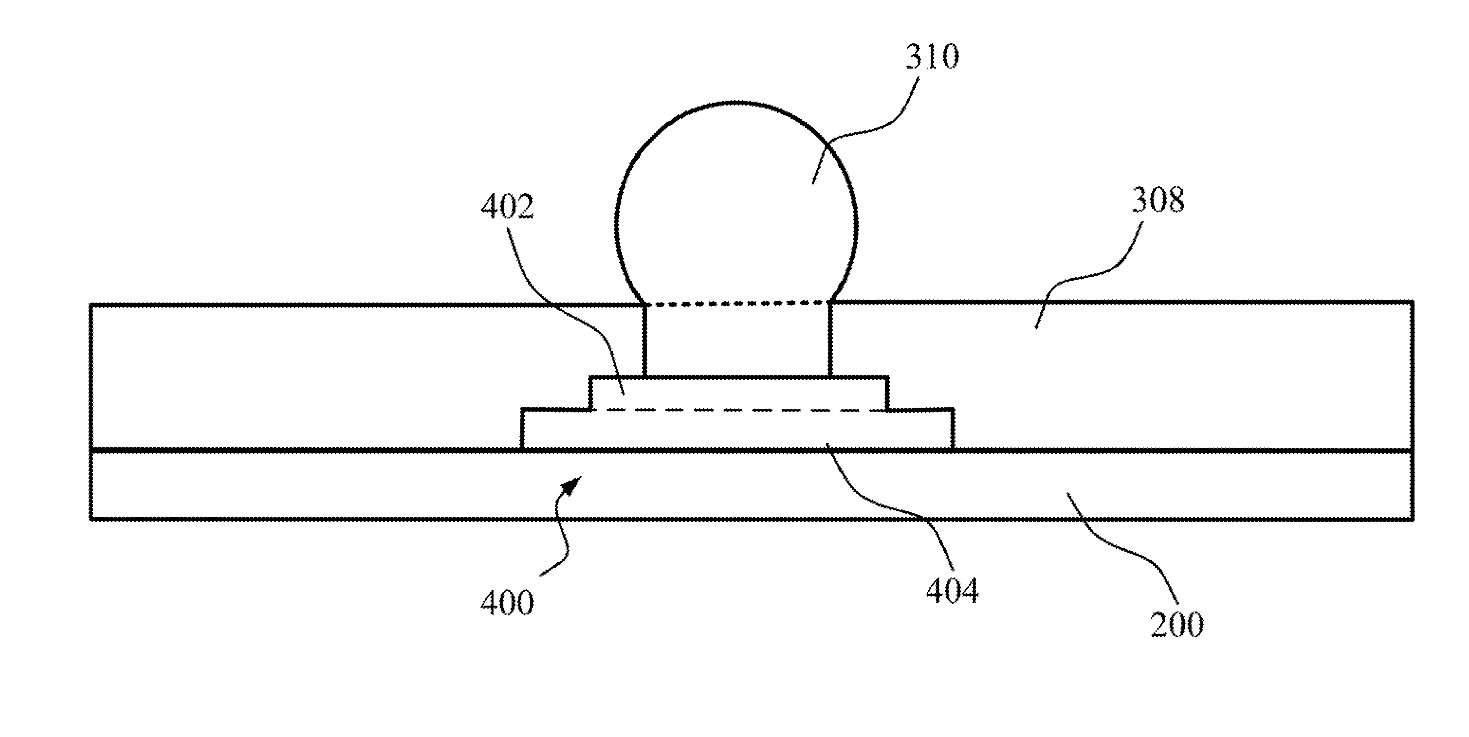
[0041]Please also refer to FIG. 4 with FIG. 6, as the metal structure is manufactured with another manufacturing method, the manufacturing method of the metal structure of the multi-layer substrate according to the present invention comprises the steps below.

[0042]A first photoresist layer 406 is coated on a first dielectric layer 200. A photolithography process is proceeded to the first photoresist layer 406 to define a first specific position for the first metal layer 400. Then, the first photoresist layer 406 at the first specific position is removed (such as a developing process). The embedded base 404 of the first metal layer 400 is formed by physical vapor deposition, like vacuum evaporation, at the first specific position. A second photoresist layer 408 is coated after the rest first photoresist layer 406 is removed. A photolithography process is proceeded to the second photoresist layer 408 at a second specific position of the first metal layer 400. Then, the second photores...


PUM

PropertyMeasurementUnit
Dielectric polarization enthalpyaaaaaaaaaa
Structureaaaaaaaaaa
Flexibilityaaaaaaaaaa

Abstract

Disclosed is a metal structure of a multi-layer substrate, comprising a first metal layer and a dielectric layer. The first metal layer has an embedded base and a main body positioned on the embedded base. The base area of the embedded base is larger than the base area of the main body. After the dielectric layer covers the main body and the embedded base, the dielectric layer is opened at the specific position of the first metal layer for connecting the first metal layer with a second metal layer above the dielectric layer. When the metal structure is employed as a pad or a metal line of the flexible multi-layer substrate according to the present invention, the metal structure cannot easily be delaminated or separated from the contacted dielectric layer. Therefore, a higher reliability for the flexible multi-layer substrate can be achieved.

Description

BACKGROUND OF THE INVENTION[0001]1. Field of the Invention[0002]The present invention generally relates to a metal structure of a multi-layer substrate and the manufacturing method thereof, and more particularly to a metal structure of a flexible multi-layer substrate and the manufacturing method thereof.[0003]2. Description of Prior Art[0004]A multi-layer substrate can be utilized for manufacturing a package substrate, a printed circuit board, a flexible package substrate or a flexible printed circuit for realizing miniaturization of all electronic products is an inevitable trend in this modern world. Particularly, a flexible multi-layer substrate can be utilized for manufacturing a flexible package structure to apply in kinds of products to meet miniaturization demands more efficiently. As the thickness of the flexible multi-layer substrate gets thinner, the routing density of the multi-layer substrate becomes higher. Accordingly, the requirements of the metal structure size of th...

Claims


Application Information

Patent Timeline
IPC IPC(8): H05K1/00H05K1/11H05K1/09G03F7/20
CPCH05K1/111H05K1/118H05K3/048H05K3/4007H05K2201/0367Y10T29/4913H05K2201/09845H05K2201/099H05K2203/0588H05K2203/0594Y10T29/49165H05K2201/098
Inventor YANG, CHIH-KUANG
Owner PRINCO CORP
Why Eureka
Try Eureka