Semiconductor device and method for manufacturing the same

Active Publication Date: 2011-04-21
SEMICON ENERGY LAB CO LTD
View PDF99 Cites 96 Cited by
  • Summary
  • Abstract
  • Description
  • Claims
  • Application Information

AI Technical Summary

Benefits of technology

[0014]By any of the above methods, an impurity such as hydrogen, moisture, hydroxyl, or hydride included in the oxide semiconductor layer is diffused into the gate insulating layer and/or the insulating layer with use of a halogen element, so that the impurity concentration in the oxide semiconductor layer is reduced.
[0015]The insulating layer preferably contains excessive oxygen a

Problems solved by technology

However, a difference from the stoichiometric composition in a

Method used


Image

  • Semiconductor device and method for manufacturing the same
  • Semiconductor device and method for manufacturing the same
  • Semiconductor device and method for manufacturing the same

Examples


Example

Embodiment 1

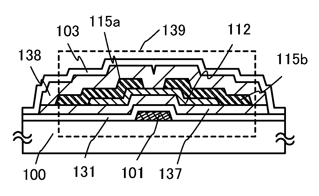
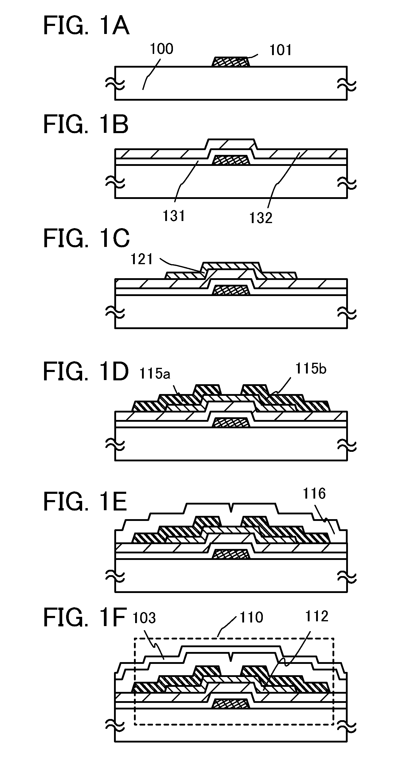
[0068]In this embodiment, one embodiment of a semiconductor device and a method for manufacturing the semiconductor device will be described with reference to FIGS. 1A to 1F. The semiconductor device described in this embodiment is a thin film transistor.

[0069]FIGS. 1A to 1F illustrate an example of a cross-sectional structure of a semiconductor device. A thin film transistor 110 illustrated in FIGS. 1A to 1F is a kind of bottom-gate structure and is also called an inverted staggered thin film transistor.

[0070]The thin film transistor 110 illustrated in FIGS. 1A to 1F includes a gate electrode layer 101, a gate insulating layer 131, a gate insulating layer 132, an oxide semiconductor layer 112, a source electrode layer 115a, and a drain electrode layer 115b over a substrate 100 having an insulating surface. In addition, an oxide insulating layer 116 which covers the thin film transistor 110 and is in contact with the oxide semiconductor layer 112 is provided, and a prote...

Example

Embodiment 2

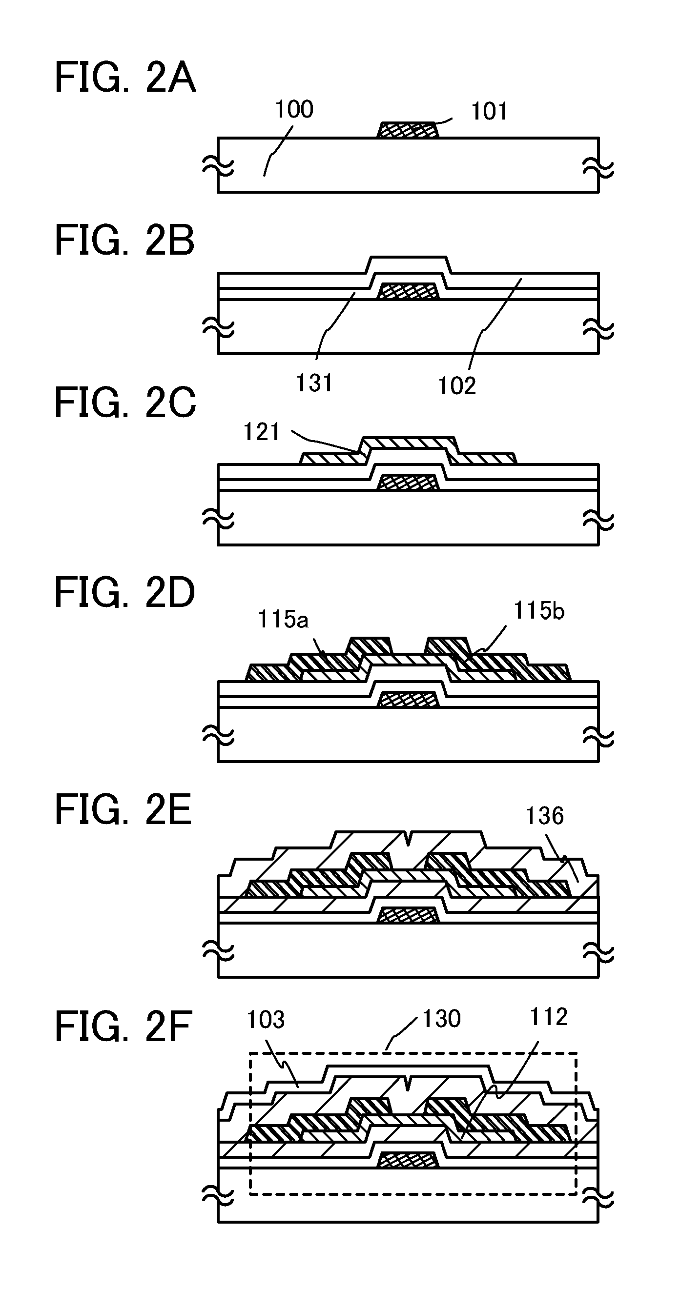
[0209]In this embodiment, another example of a thin film transistor applicable to a semiconductor device disclosed in this specification will be described. The same portion as or a portion having a function similar to those described in the above Embodiment 1 can be formed in a manner similar to that described in Embodiment 1, and also the steps similar to those of Embodiment 1 can be performed in a manner similar to those described in Embodiment 1; therefore, repetitive description is omitted. Detailed description of the same portions is omitted.

[0210]FIGS. 2A to 2F illustrate an example of a cross-sectional structure of a semiconductor device. A thin film transistor 130 illustrated in FIGS. 2A to 2F is a kind of bottom-gate structure and is also called an inverted staggered thin film transistor.

[0211]The thin film transistor 130 illustrated in FIGS. 2A to 2F includes a gate electrode layer 101, a gate insulating layer 131, a gate insulating layer 102, an oxide semicond...

Example

Embodiment 3

[0243]In this embodiment, another example of a thin film transistor applicable to a semiconductor device disclosed in this specification will be described. The same portion as or a portion having a function similar to those described in the above embodiments can be formed in a manner similar to that described in the above embodiments, and also the steps similar to those of the above embodiments can be performed in a manner similar to those described in the above embodiments; therefore, repetitive description is omitted. Detailed description of the same portions is omitted.

[0244]FIGS. 3A to 3F illustrate an example of a cross-sectional structure of a semiconductor device. A thin film transistor 135 illustrated in FIGS. 3A to 3F is a kind of bottom-gate structure and is also called an inverted staggered thin film transistor.

[0245]The thin film transistor 135 illustrated in FIGS. 3A to 3F includes a gate electrode layer 101, a gate insulating layer 131, a gate insulating la...


PUM


Abstract

An object is to provide a semiconductor device with stable electric characteristics in which an oxide semiconductor is used. An impurity such as hydrogen or moisture (e.g., a hydrogen atom or a compound containing a hydrogen atom such as H2O) is eliminated from an oxide semiconductor layer with use of a halogen element typified by fluorine or chlorine, so that the impurity concentration in the oxide semiconductor layer is reduced. A gate insulating layer and/or an insulating layer provided in contact with the oxide semiconductor layer can be formed to contain a halogen element. In addition, a halogen element may be attached to the oxide semiconductor layer through plasma treatment under an atmosphere of a gas containing a halogen element.

Description

TECHNICAL FIELD[0001]The present invention relates to a semiconductor device including an oxide semiconductor and a method for manufacturing the semiconductor device.[0002]Note that the semiconductor devices in this specification indicate all the devices which can operate by using semiconductor characteristics, and an electronic optical device, a semiconductor circuit, and an electronic device are all included in the semiconductor devices.BACKGROUND ART[0003]A technique for forming a thin film transistor (TFT) by using a semiconductor thin film formed over a substrate having an insulating surface has attracted attention. A thin film transistor is used for a display device typified by a liquid crystal television device. A silicon-based semiconductor material is known as a semiconductor thin film that can be applied to a thin film transistor, and in addition, an oxide semiconductor has attracted attention as another material that can be applied to a thin film transistor.[0004]As a mat...

Claims


Application Information

Patent Timeline
IPC IPC(8): H01L29/12H01L21/34
CPCH01L21/02554H01L21/02565H01L21/02631H01L29/4908H01L29/78606H01L21/02664H01L29/66969H01L2924/0002H01L29/7869H01L23/564H01L2924/00H01L29/66742H01L21/02266
Inventor YAMAZAKI, SHUNPEISUZUKI, KUNIHIKOTAKAHASHI, MASAHIRO
Owner SEMICON ENERGY LAB CO LTD
Why Eureka
Try Eureka