Semiconductor device

Active Publication Date: 2014-10-16
SEMICON ENERGY LAB CO LTD
View PDF16 Cites 27 Cited by
  • Summary
  • Abstract
  • Description
  • Claims
  • Application Information

AI Technical Summary

Benefits of technology

[0023]According to one embodiment of the present invention, the stability of a step of processing a wiring formed using copper, aluminum, gold, silver, molybdenum, or the like can be increased. Further, according to one embodiment of the present invention, in a semiconductor device or the like including an oxide semiconductor film, the concentration of impurities in the oxide semiconductor film can be reduced. Further, according to one embodiment of the present invention, in a semiconductor device including an oxide semiconductor film, electrical characteristics ca

Problems solved by technology

However, there are problems in that copper, aluminum, gold, silver, molybdenum, or the like, which is a constituent element of the wiring, is difficult to process, and they are diffused in an oxide semiconductor film in the course of the processing.
Copper, aluminum, gold, silver, molybdenum, or the like, which is a constituent element of the wiring, is one of impuri

Method used


Image

  • Semiconductor device
  • Semiconductor device
  • Semiconductor device

Examples


embodiment 1

[0064]In this embodiment, a semiconductor device which is one embodiment of the present invention and a manufacturing method thereof are described with reference to drawings.

[0065]In a transistor including an oxide semiconductor film, oxygen vacancies are given as an example of a defect which leads to poor electrical characteristics of the transistor. For example, the threshold voltage of a transistor including an oxide semiconductor film which contains oxygen vacancies in the film easily shifts in the negative direction, and such a transistor tends to have normally-on characteristics. This is because electric charges are generated owing to oxygen vacancies in the oxide semiconductor film and the resistance is thus reduced. The transistor having normally-on characteristics causes various problems in that malfunction is likely to be caused when in operation and that power consumption is increased when not in operation. Further, there is a problem in that the amount of change in elect...

modification example 2

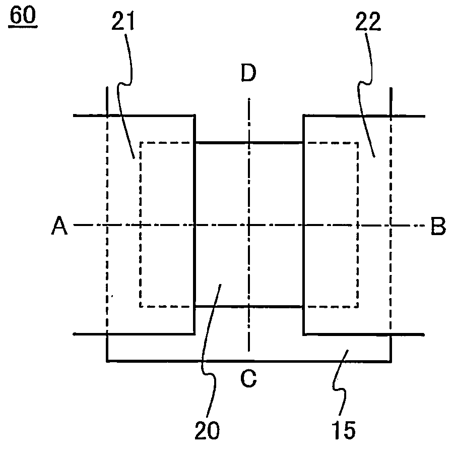
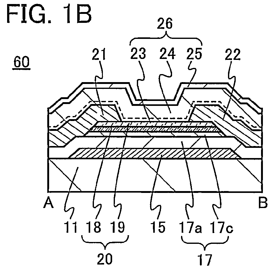
[0262]As for the pair of electrodes 21 and 22 provided in the transistor 60 described in this embodiment, it is preferable to use a conductive material which is easily bonded to oxygen, such as copper, aluminum, and molybdenum, or an alloy thereof. Thus, oxygen contained in the multilayer film 20 and the conductive material contained in the pair of electrodes 21 and 22 are bonded to each other, so that an oxygen deficient region is formed in the multilayer film 20. Further, in some cases, part of constituent elements of the conductive material that forms the pair of electrodes 21 and 22 is mixed into the multilayer film 20. Consequently, low-resistance regions are formed in the vicinity of regions of the multilayer film 20 which are in contact with the pair of electrodes 21 and 22. The low-resistance regions are formed between the gate insulating film 17 and the pair of electrodes 21 and 22 so as to be in contact with the pair of electrodes 21 and 22. Since the low-resistance region...

modification example 3

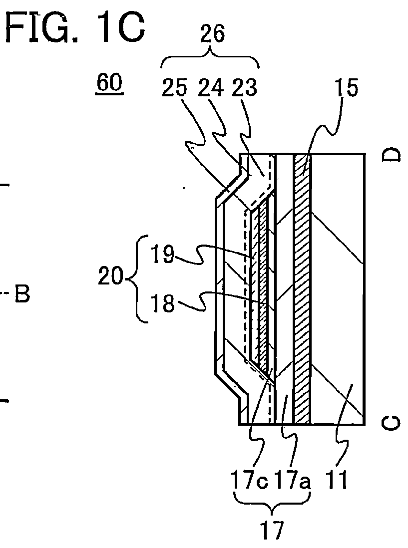
[0264]As illustrated in FIG. 15, over the transistor 60 in this embodiment, a protective film 26a in which the oxide insulating film 24 and the nitride insulating film 25 are stacked can be provided. In the transistor in FIG. 15, the oxide film 19 is provided over the oxide semiconductor film 18; thus, the oxide film 19 functions as a protective film at the time of formation of the oxide insulating film 24. As a result, when the oxide insulating film 24 is formed, the oxide semiconductor film 18 is not exposed to plasma, and plasma damage which is generated at the time of forming the oxide insulating film 24 by a plasma CVD method with relatively high power can be reduced.

[0265]Further, oxygen contained in the oxide insulating film 24 can be directly transferred to the multilayer film 20; thus, the amount of oxygen supplied to the oxide semiconductor film 18 can be increased. As a result, the number of oxygen vacancies in the oxide semiconductor film 18 can be further reduced.

[0266]...


PUM


Abstract

The stability of a step of processing a wiring formed using copper, aluminum, gold, silver, molybdenum, or the like is increased. Moreover, the concentration of impurities in a semiconductor film is reduced. Moreover, the electrical characteristics of a semiconductor device are improved. In a transistor including an oxide semiconductor film, an oxide film in contact with the oxide semiconductor film, and a pair of conductive films being in contact with the oxide film and including copper, aluminum, gold, silver, molybdenum, or the like, the oxide film has a plurality of crystal parts and has c-axis alignment in the crystal parts, and the c-axes are aligned in a direction parallel to a normal vector of a top surface of the oxide semiconductor film or the oxide film.

Description

BACKGROUND OF THE INVENTION[0001]1. Field of the Invention[0002]The present invention relates to a semiconductor device including a transistor and a manufacturing method thereof.[0003]2. Description of the Related Art[0004]Transistors used for most flat panel displays typified by a liquid crystal display device or a light-emitting display device are formed using a silicon semiconductor such as amorphous silicon, single crystal silicon, or polycrystalline silicon provided over a glass substrate. Further, such a transistor employing such a silicon semiconductor is used in integrated circuits (ICs) and the like.[0005]In recent years, attention has been drawn to a technique in which, instead of a silicon semiconductor, a metal oxide exhibiting semiconductor characteristics is used in transistors. Note that in this specification, a metal oxide exhibiting semiconductor characteristics is referred to as an oxide semiconductor.[0006]For example, such a technique is disclosed that a transist...

Claims


Application Information

Patent Timeline
IPC IPC(8): H01L27/12H01L29/786
CPCH01L29/7869H01L27/1225H01L29/78696G02F1/1362G02F1/133345H01L29/045H01L27/1229H01L29/04H01L21/02609H01L29/66969
Inventor YAMAZAKI, SHUNPEIKOEZUKA, JUNICHINAKAZAWA, YASUTAKASHIMA, YUKINORIJINTYOU, MASAMISAKAKURA, MASAYUKINAKASHIMA, MOTOKI
Owner SEMICON ENERGY LAB CO LTD
Why Eureka
Try Eureka