Semiconductor device mounted structure and its manufacturing method

Active Publication Date: 2011-04-28
PANASONIC CORP
View PDF7 Cites 23 Cited by
  • Summary
  • Abstract
  • Description
  • Claims
  • Application Information

AI Technical Summary

Benefits of technology

[0038]In the semiconductor device mounted structure according to the present invention, because the plurality of reinforcing resin members are respectively positioned around the bonding members so as to cover at least the bonding members and bonding regions between the bonding members and the bumps, the bonding members and the bonding regions between the bonding members and the bumps can be positively reinforced by the reinforcing resin members. Also, because the reinforcing resin members are positioned so as to cover the bonding members and the bonding regions between the bonding members and the bumps without being in contact with the semiconductor device, repairs to the semiconductor device mounted structure can be easily carried out, compared with a conventional structure in which a space between t

Problems solved by technology

However, the reliability in BGA connection with the use of the Sn—Zn-bas

Method used


Image

  • Semiconductor device mounted structure and its manufacturing method
  • Semiconductor device mounted structure and its manufacturing method
  • Semiconductor device mounted structure and its manufacturing method

Examples


first embodiment

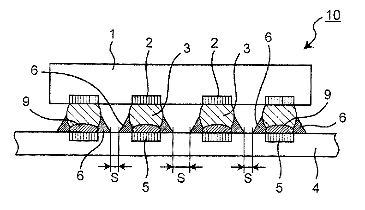
[0050]FIG. 1 is a schematic partial sectional view of a structure 10 on which a semiconductor package 1 obtained by a mounting method according to a first embodiment of the present invention has been mounted. The term “semiconductor package” as employed throughout this application is defined as an example of a semiconductor device and includes a single semiconductor device or a package having a semiconductor device. As shown in FIG. 1, the semiconductor package-mounted structure 10 includes a BGA semiconductor package 1 having a plurality of electrodes 2, a plurality of solder bumps 3 each formed on one of the electrodes 2, a circuit board 4 having a plurality of board electrodes (an example of a second electrode) 5, a plurality of bonding members 9 each interposed between one of the solder bumps 3 and an associated one of the board electrodes 5 for electrical connection thereof, and a plurality of reinforcing resins (reinforcing resinous members) 6 each formed around one of the bon...

second embodiment

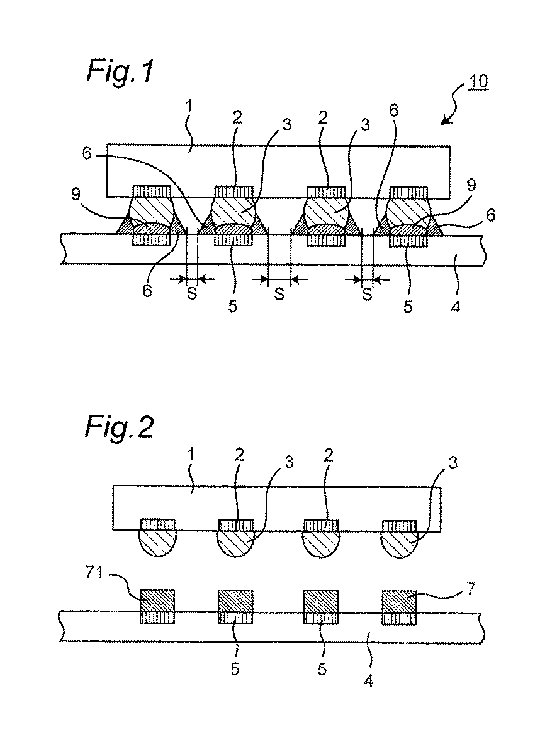
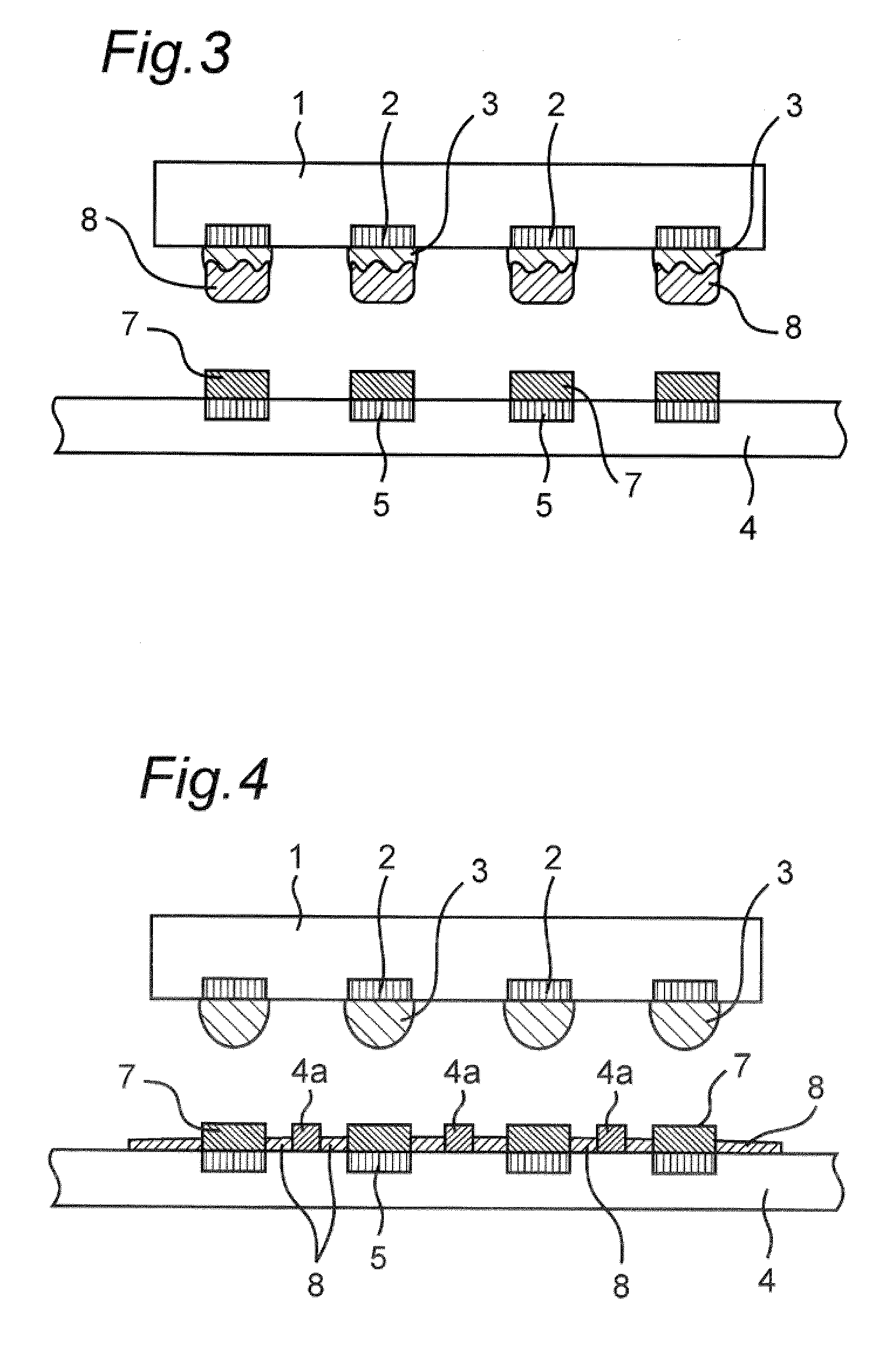
[0064]The second embodiment pertains to a mounting method for a semiconductor package 1 embodying one form of the present invention, i.e., a manufacturing method of the semiconductor package-mounted structure 10. Three patterns of mounting methods (manufacturing methods) are explained with reference to FIGS. 2, 3 and 4, respectively. Component parts that are substantially the same as those of the structure 10 shown in FIG. 1 are designated by the same reference numerals, and explanation thereof is omitted for the sake of brevity.

(First Mounting Method)

[0065]The first mounting method is first explained. As shown in FIG. 2, a pattern of mixed paste 71 (mixed paste in which a soldering material and a thermosetting resin have been mixed) is printed on the board electrodes 5 of the circuit board 4. A typical example of the mixed paste includes a soldering material of alloy composition consisting of a combination of Sn and one or more elements selected from the group consisting of Bi, In,...

example

[0076]The impact resistance and the repairing capability of the structure 10 in which the BGA semiconductor package 1 has been incorporated using the above-described second mounting method were investigated by changing the kind of the soldering paste, the reflow temperature, and the amount of the reinforcing resin. FIG. 5 is a table indicating results of the investigation and particularly indicating examples 1-6 of the structure 10 according to the second mounting method and comparative examples 1-4 for comparison.

[0077]As the soldering paste 7, an Sn58Bi soldering paste (trade name “L20-BLT-5-T7F”, made by Senju Metal Industry Co., Ltd.) was used. The following were also commonly used.

[0078]BGA semiconductor package 1: semiconductor package having daisy chain connection and SnAgCu balls employed as solder bumps 3

[0079]Thermosetting resin: bisphenol F-type epoxy resin (trade name “epicort 806”, made by Japan Epoxy Resins Co., Ltd.)

[0080]Curing agent: imidazole curing agent (trade na...


PUM


Abstract

A semiconductor device mounted structure includes a semiconductor device having a plurality first electrodes, a circuit board having a plurality of second electrodes, a plurality of bumps respectively formed on the plurality of first electrodes, a plurality of bonding members respectively positioned between the bumps and the second electrodes to electrically connect the first electrodes to the second electrodes via the bumps, and a plurality of reinforcing resin members respectively positioned around the bonding members so as to cover at least the bonding members and bonding regions between the bonding members and the bumps. Adjacent reinforcing resin members are spaced away from each other so as not to have contact with each other without being in contact with the semiconductor device. This semiconductor device mounted structure enhances the reliability of joints in impact resistance and makes it easy to repair it.

Description

TECHNICAL FIELD[0001]The present invention relates to a semiconductor device mounted structure in which a semiconductor device such as, for example, a semiconductor chip (semiconductor element) or a semiconductor package is electrically connected to a circuit board. The present invention also relates to a manufacturing method of the semiconductor device mounted structure.BACKGROUND ART[0002]Mobile devices such as mobile phones, PDAs (Personal Digital Assistants), and the like are nowadays progressively reduced in size and sophisticated, and a mounted structure such as a BGA (Ball Grid Array) or CSP (Chip Scale Package) is widely used to respond to such a trend. Because the mobile devices are susceptible to mechanical load such as drop impact, it is important for the mounted structure such as a BGA or CSP not having any impact relieving structure such as leads of a QFP (Quad Flat Package) to ensure the reliability of soldered joints in impact resistance.[0003]In soldering, for exampl...

Claims


Application Information

Patent Timeline
IPC IPC(8): H01L23/498H01L21/60
CPCH01L21/563H01L2224/13111H01L23/49894H01L24/12H01L24/16H01L24/81H01L2224/10126H01L2224/13099H01L2224/73203H01L2224/812H01L2224/81801H01L2224/83192H01L2224/83194H01L2224/83855H01L2224/83856H01L2924/01004H01L2924/01013H01L2924/01027H01L2924/01029H01L2924/0103H01L2924/01033H01L2924/01049H01L2924/01075H01L2924/01079H01L2924/01082H05K3/3436H05K3/3452H05K3/3463H05K3/3484H05K2201/10977H05K2201/10992H01L2924/01006H01L2924/01047H01L2924/014H01L2224/16225H01L2224/13566H01L2224/16058H01L23/49816H01L2224/13109H01L2224/131H01L2924/01083H01L2924/00014H01L2924/0105H05K3/3485Y02P70/50
Inventor OHASHI, NAOMICHISAKATANI, SHIGEAKIKISHI, ARATAYAMAGUCHI, ATSUSHIMIYAKAWA, HIDENORI
Owner PANASONIC CORP
Why Eureka
Try Eureka