Normally off gallium nitride field effect transistors (FET)

a field effect transistor and gallium nitride technology, applied in transistors, semiconductor devices, instruments, etc., can solve the problems of increased power consumption, complicated devices, and devices that are not suitable for those applications, and achieve simple and convenient manufacturing and operating processes, improve device configuration, and improve the effect of device configuration

Active Publication Date: 2011-05-05
ALPHA & OMEGA SEMICON INC
View PDF3 Cites 22 Cited by
  • Summary
  • Abstract
  • Description
  • Claims
  • Application Information

AI Technical Summary

Benefits of technology

[0009]It is therefore an aspect of the present invention to provide a new and improved device configuration and manufacturing method to provide a heterostructure field effect transistor (HFET) power device that provides simple and convenient manufacturing and operating processes to implement the HFET device as a normally-off device such that the above discussed difficulties and limitations may be resolved.
[0010]Specifically, it is an aspect of the present invention to provide improved device configuration and method for manufacturing a semiconductor GaN-based HFET power device with negatively charged floating gate to deplete the channel when no voltage is applied to the gate. The negative charged floating gate is formed by applying a similar process as for forming a floating gate commonly implemented in flash memory, which is a mature and well known technology. A gate voltage is applied to offset the negatively charged floating gate to restore the 2DEG channel formed on the hetero-junction between the GaN and AlGaN layers.
[0011]It is another aspect of the present invention to provide improved device configuration and method for manufacturing a multiple-channel semiconductor GaN-based HFET power device with negatively charged floating gate formed as wrap-around floating gate to deplete the multiple channels when no voltage is applied to the gate. The negative charged floating gate is provided by applying a similar process as a floating gate commonly implemented in flash memory. A gate voltage is applied to offset the negatively charged wrap-around floating gate to restore the 2DEG channels formed on the hetero-junctions between multiple layers of GaN and AlGaN interfaces.
[0012]It is another aspect of the present invention to provide improved device configuration and method for manufacturing a semiconductor GaN-based HFET power device with negatively charged gate oxide layer to deplete the channel when no voltage is applied to the gate. The negative charged gate oxide may be provided by fluorine treatment or a similar process to deposit fixed negative charges into the gate oxide layer. A gate voltage is applied to offset the negatively charged gate oxide to restore the 2DEG channel formed on the hetero-junction between the GaN and AlGaN layers.
[0013]Briefly in a preferred embodiment this invention discloses a heterostructure field effect transistor (HFET) gallium nitride (GaN) semiconductor power device. The power device comprises a hetero junction structure comprises a first semiconductor layer interfacing a second semiconductor layer of two different band gaps thus generating an interface layer as a two-dimensional electron gas (2DEG) layer. The power device further comprises a source electrode and a drain electrode disposed on two opposite sides of a gate electrode disposed on top of the hetero-junction structure for controlling a current flow between the source and drain electrodes in the 2DEG layer. The power device further comprises a floating gate loc

Problems solved by technology

Conventional methods of configuring and manufacturing a gallium nitride (GaN) based field effect transistors (FETs) are still continuously challenged with a technical issue for providing a normally-off FET transistor that has simple and convenient manufacturing and operating configurations.
A requirement to continuous apply a pinch off voltage to the gate in order to turn off the transistor thus leads to additional power consumptions and may often cause a more complicated device control process for implementing such transistor in an electronic device.
In addition most applications are design

Method used


Image

  • Normally off gallium nitride field effect transistors (FET)
  • Normally off gallium nitride field effect transistors (FET)
  • Normally off gallium nitride field effect transistors (FET)

Examples


Embodiment Construction

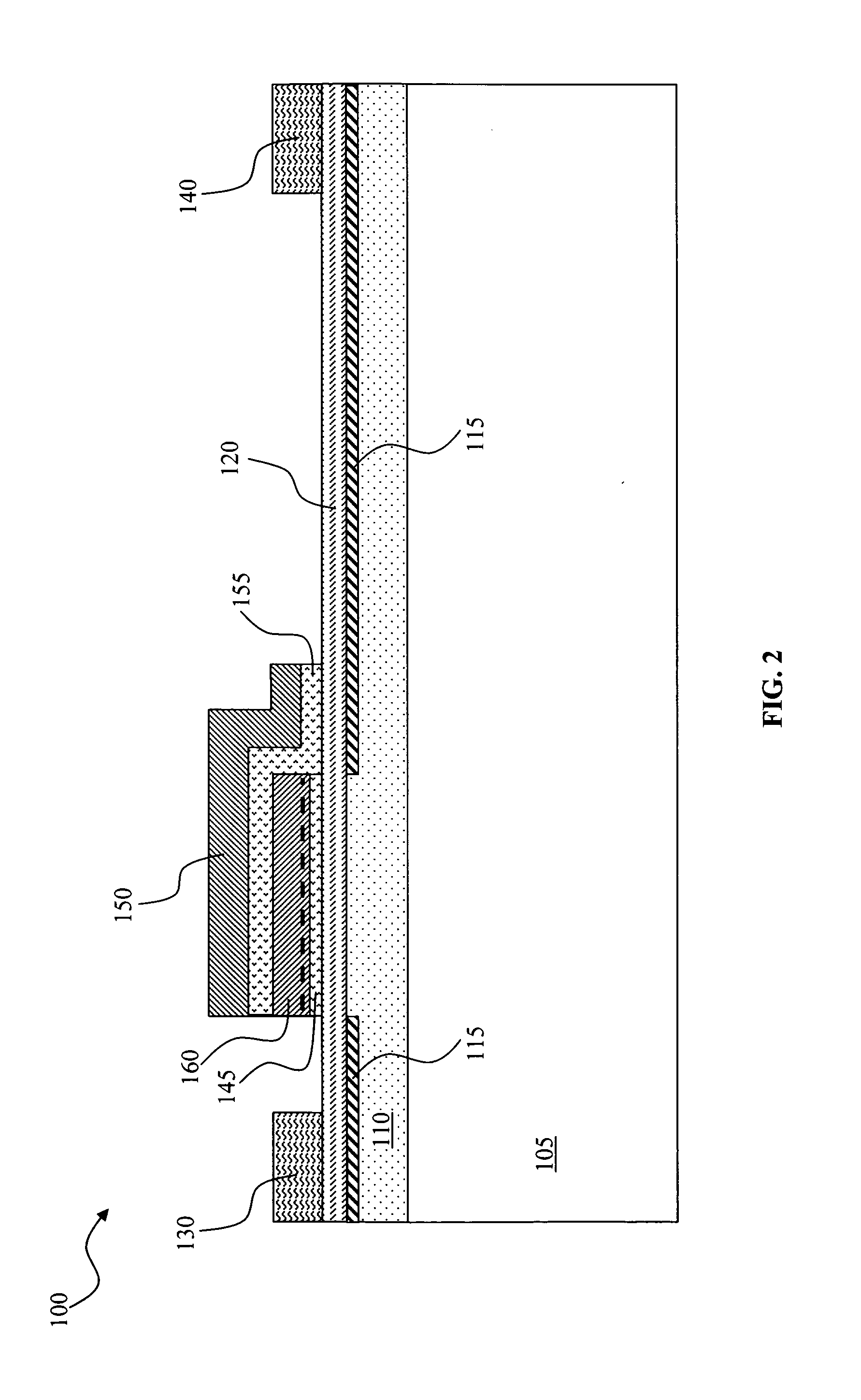
[0021]Referring to FIG. 2 for a cross sectional view of a heterostructure field effect transistor (HFET) semiconductor power device 100 of this invention. The HFET semiconductor power device 100 comprises an AlGaN layer 120 epitaxial grown on top of gallium nitride (GaN) layer 110 thus forming a AlGaN / GaN hetero-junction with a two-dimensional electron gas (2DEG) 115 located at the interface. The AlGaN / GaN hetero junction structure is supported on a sapphire substrate 105. A source electrode 130 and a drain 140 are disposed on two opposite sides of a gate electrode 150 to control the current flow through the 2DEG layer 115. The gate electrode 150 is insulated from the N-doped AlGaN layer 120 with a thicker gate oxide layer 155. In order to configure the HFET power device as a normally off device, a floating gate 160 is formed beneath at least a portion of the gate oxide layer 155. The floating gate 160 is insulated from the AlGaN layer 120 with a thin oxide layer 145, and from the g...


PUM


Abstract

A heterostructure field effect transistor (HFET) gallium nitride (GaN) semiconductor power device comprises a hetero-junction structure comprises a first semiconductor layer interfacing a second semiconductor layer of two different band gaps thus generating an interface layer as a two-dimensional electron gas (2DEG) layer. The power device further comprises a source electrode and a drain electrode disposed on two opposite sides of a gate electrode disposed on top of the hetero-junction structure for controlling a current flow between the source and drain electrodes in the 2DEG layer. The power device further includes a floating gate located between the gate electrode and hetero-junction structure, wherein the gate electrode is insulated from the floating gate with an insulation layer and wherein the floating gate is disposed above and padded with a thin insulation layer from the hetero-junction structure and wherein the floating gate is charged for continuously applying a voltage to the 2DEG layer to pinch off the current flowing in the 2DEG layer between the source and drain electrodes whereby the HFET semiconductor power device is a normally off device.

Description

BACKGROUND OF THE INVENTION[0001]1. Field of the Invention[0002]The invention relates generally to the configurations and methods of manufacturing the semiconductor devices. More particularly, this invention relates to a gallium nitride (GaN)-based field effect transistor implemented with new device configurations and manufacturing methods for a normally-off GaN-based field effect transistor that has an extremely small ON resistance in conducting a large amount of electric current.[0003]2. Description of the Prior Art[0004]Conventional methods of configuring and manufacturing a gallium nitride (GaN) based field effect transistors (FETs) are still continuously challenged with a technical issue for providing a normally-off FET transistor that has simple and convenient manufacturing and operating configurations. Specifically, gallium nitride (GaN) based FETs have been implemented to make high electron mobility transistors (HEMTs). For applications of the power transistors, this type of...

Claims


Application Information

Patent Timeline
IPC IPC(8): G11C16/04H01L31/00H01L21/337
CPCH01L29/1029H01L29/2003H01L29/402H01L29/785H01L29/66462H01L29/7787H01L29/41725
Inventor BHALLA, ANUPZHU, TINGGANG
Owner ALPHA & OMEGA SEMICON INC
Why Eureka
Try Eureka