Solid-state imaging device, manufacturing method and designing method thereof, and electronic device

a technology of solid-state imaging and manufacturing methods, applied in the direction of optical radiation measurement, radiation controlled devices, instruments, etc., can solve problems such as difficult suppression, and achieve the effect of suppressing color non-uniformity and reducing the variation in the optical interference intensity of incident light on the light-receiving surfa

Active Publication Date: 2011-05-12
SONY SEMICON SOLUTIONS CORP
View PDF26 Cites 29 Cited by
  • Summary
  • Abstract
  • Description
  • Claims
  • Application Information

AI Technical Summary

Benefits of technology

[0042]According to an embodiment of the present invention, there is provided a solid-state imaging device that includes: a semiconductor substrate that includes a photodiode separately provided for each of pixels disposed in a matrix on a light-receiving surface; a first insulating film formed on the semiconductor substrate so as to cover multilayer wiring formed on and in contact with the semiconductor substrate, wherein the first insulating film is formed using material of a first refractive index lower than a refractive index of the semiconductor substrate for at least bottom surface and top surface portions of the first insulating film; a second insulating film of a second refractive index higher than the first refractive index formed on the first insulating film; a third insulating film of a third refractive index higher than the second refractive index formed on the second insulating film; and a color filter formed on the third insulating film in a corresponding manner with each pixel so as to transmit light in a wavelength region of red, green, or blue, wherein the thickness and / or the second refractive index of the second insulating film for a pixel with the color filter of red, green, or blue differ from the thickness and / or the second refractive index of the second insulating film for the other pixels so as to reduce variation in the intensity of optical interference between reflected light at a surface of the semiconductor substrate, and reflected light at the interfaces between the first insulating film and the second insulating film and between the second insulating film and the third insulating film.
[0057]With the electronic device according to the embodiment of the present invention, variation in the optical interference intensity of the incident light on the light-receiving surface can be reduced to suppress color nonuniformity, for example, in an electronic device that includes the generation of solid-state imaging device that forms color images particularly with a cell pitch of 3 μm or less.

Problems solved by technology

The present inventors have recognized a problem in the solid-state imaging devices of related art, specifically, difficulties in suppressing color nonuniformity, for example, in the generation of solid-state imaging device that forms color images particularly with a cell pitch of 3 μm or less.

Method used


Image

  • Solid-state imaging device, manufacturing method and designing method thereof, and electronic device
  • Solid-state imaging device, manufacturing method and designing method thereof, and electronic device
  • Solid-state imaging device, manufacturing method and designing method thereof, and electronic device

Examples


first embodiment

Configuration of Solid-State Imaging Device

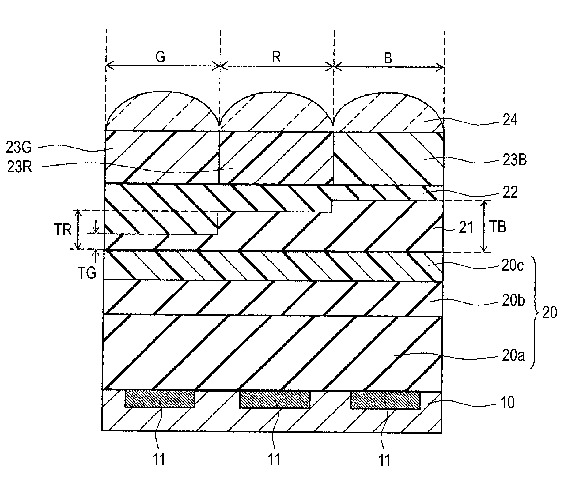
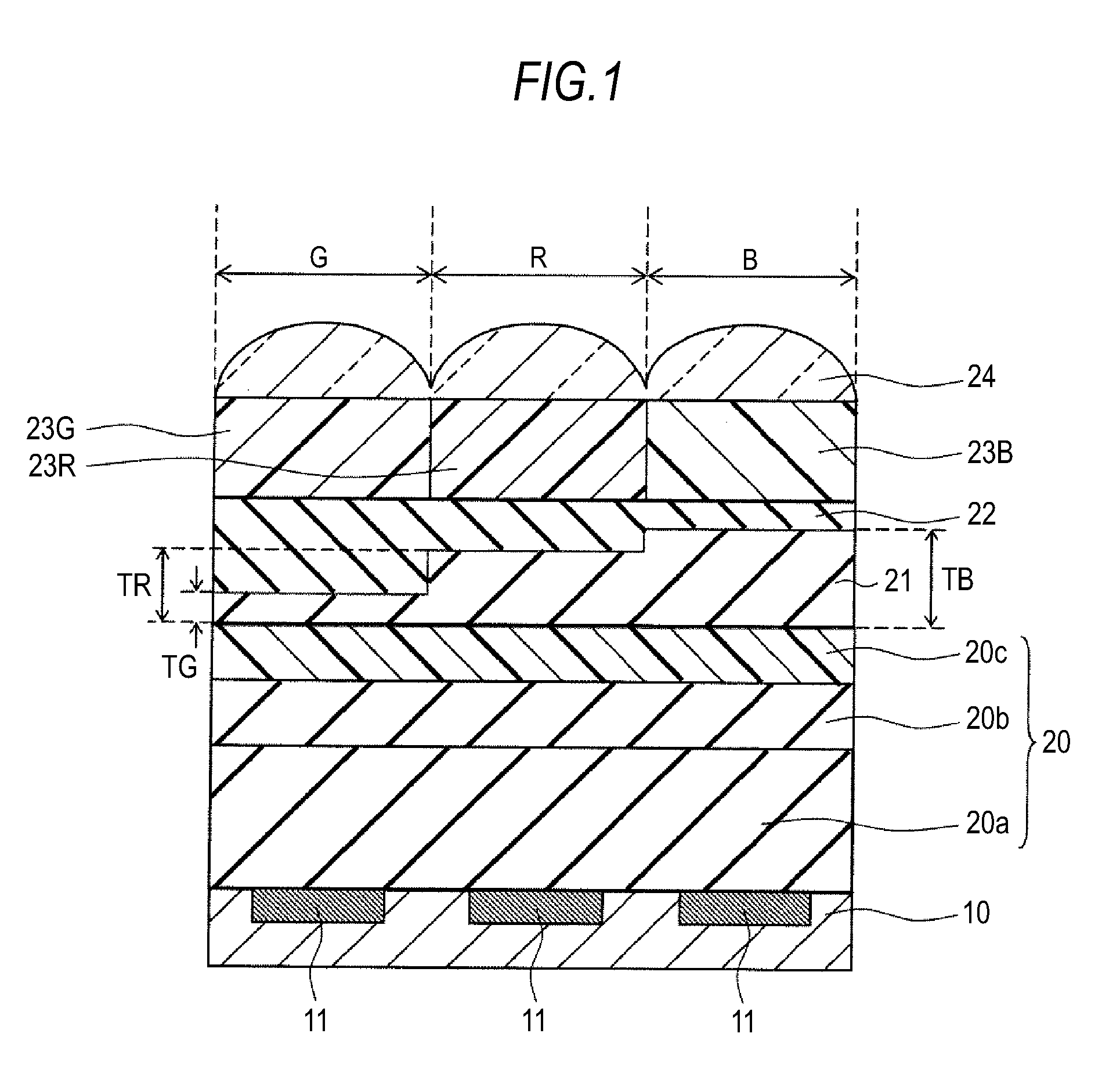
[0089]FIG. 1 is cross sectional view of pixels of a solid-state imaging device according to the present embodiment.

[0090]The figure shows a red pixel (R), a green pixel (G), and a blue pixel (B) that receive, for example, the wavelengths of the red, green, and blue regions, respectively.

[0091]For example, the red pixel (R), the green pixel (G), and the blue pixel (B) receive the wavelengths of 620 nm, 550 nm, and 440 nm, respectively.

[0092]A photodiode 11 is formed for each pixel of a semiconductor substrate 10, and a gate insulating film of, for example, silicon oxide, and gate electrodes of, for example, polysilicon, are formed on the semiconductor substrate 10 in regions adjacent to the photodiodes 11. For example, transistors are formed for the transfer of signal charges that accumulate in the photodiodes.

[0093]In the present embodiment, the photodiodes are also called sensors, and the output intensity of the photodiodes is also referre...

second embodiment

Configuration of Solid-State Imaging Device

[0161]The solid-state imaging device according to the present embodiment is essentially the same as that described in First Embodiment.

[0162]FIG. 6 represents the relationship between the sensor intensity of the red pixel (R) and the thickness of the middle-layer first insulating film 20b under varying thicknesses of the second insulating film 21 over the range of 40 nm to 455 nm.

[0163]FIG. 7 represents the relationship between the sensor intensity of the green pixel (G) and the thickness of the middle-layer first insulating film 20b under varying thicknesses of the second insulating film 21 over the range of 40 nm to 455 nm.

[0164]FIG. 8 represents the relationship between the sensor intensity of the green pixel (G) and the thickness of the middle-layer first insulating film 20b under varying thicknesses of the second insulating film 21 over the range of 5 nm to 40 nm.

[0165]FIG. 9 represents the relationship between the sensor intensity of ...

third embodiment

Configuration of Solid-State Imaging Device

[0185]FIG. 11 is a cross sectional view of pixels of a solid-state imaging device according to the present embodiment.

[0186]The second insulating film 21 is configured as the laminate of three layers: a bottom-layer second insulating film 21a, a middle-layer second insulating film 21b, and a top-layer second insulating film 21c.

[0187]The other configuration is essentially the same as the solid-state imaging device of First Embodiment.

[0188]With the solid-state imaging device of the present embodiment, variation in the optical interference intensity of the incident light on the light-receiving surface can be reduced to suppress color nonuniformity, for example, in the generation of solid-state imaging device that forms color images particularly with a cell pitch of 3 μm or less.

[0189]The bottom-layer second insulating film 21a, the middle-layer second insulating film 21b, and the top-layer second insulating film 21c may be formed using the ...


PUM


Abstract

A solid-state imaging device includes: a semiconductor substrate that includes a photodiode separately provided for each of pixels disposed in a matrix on a light-receiving surface; a first insulating film formed on the semiconductor substrate so as to cover multilayer wiring formed on and in contact with the semiconductor substrate, wherein the first insulating film is formed using material of a first refractive index lower than a refractive index of the semiconductor substrate for at least bottom surface and top surface portions of the first insulating film; a second insulating film of a second refractive index higher than the first refractive index formed on the first insulating film; a third insulating film of a third refractive index higher than the second refractive index formed on the second insulating film; and a color filter formed on the third insulating film in a corresponding manner with each pixel so as to transmit light in a wavelength region of red, green, or blue.

Description

BACKGROUND OF THE INVENTION[0001]1. Field of the Invention[0002]The present invention relates to solid-state imaging devices, manufacturing methods and designing methods thereof, and electronic devices, particularly to solid-state imaging devices that include R (red), G (green), and B (blue) color filters, manufacturing methods and designing methods thereof, and electronic devices.[0003]2. Description of the Related Art[0004]Electronic devices such as digital video electronic devices and digital still electronic devices include solid-state imaging devices, for example, such as CCD (Charge Coupled Device) image sensors, and CMOS (Complementary Metal-Oxide-Silicon Transistor) image sensors.[0005]Such solid-state imaging devices include a plurality of pixels that is disposed in a matrix along the horizontal and vertical directions to form a light-receiving surface on a semiconductor substrate. On the light-receiving surface, a sensor, for example, such as a photodiode, is provided as a...

Claims


Application Information

Patent Timeline
Patent Type & Authority Applications(United States)
IPC IPC(8): H01L27/146H01L31/0232H01L31/18
CPCH01L27/14621H01L27/14632H01L27/14645H01L31/0232H01L27/14687H01L27/14689H01L27/14685
Inventor IZUHA, KYOKOOKAZAKI, HIROMIKITANO, YOSHIAKI
Owner SONY SEMICON SOLUTIONS CORP
Why Eureka
Try Eureka