Semiconductor device and information processing system

a technology of information processing system and semiconductor device, which is applied in the direction of voltage/current interference elimination, oscillation generator, reliability increasing modifications, etc., can solve the problems of inability to obtain a good signal quality at a high data transmission rate, inability to perform correct signal transmission and reception, etc., and achieve the effect of reducing power consumption

Active Publication Date: 2011-05-12
LONGITUDE LICENSING LTD
View PDF4 Cites 38 Cited by
  • Summary
  • Abstract
  • Description
  • Claims
  • Application Information

AI Technical Summary

Benefits of technology

[0013]According to the present invention, because a rising time and a falling time of an output signal are maintained by means of a characteristic switching circuit, an increase in an influence of a harmonic component, a crosstalk, or reflection when a power voltage is redu

Problems solved by technology

Due to this, transmission and reception of signals cannot be performed correctly.
As a result, because a propagation w

Method used


Image

  • Semiconductor device and information processing system
  • Semiconductor device and information processing system
  • Semiconductor device and information processing system

Examples


first embodiment

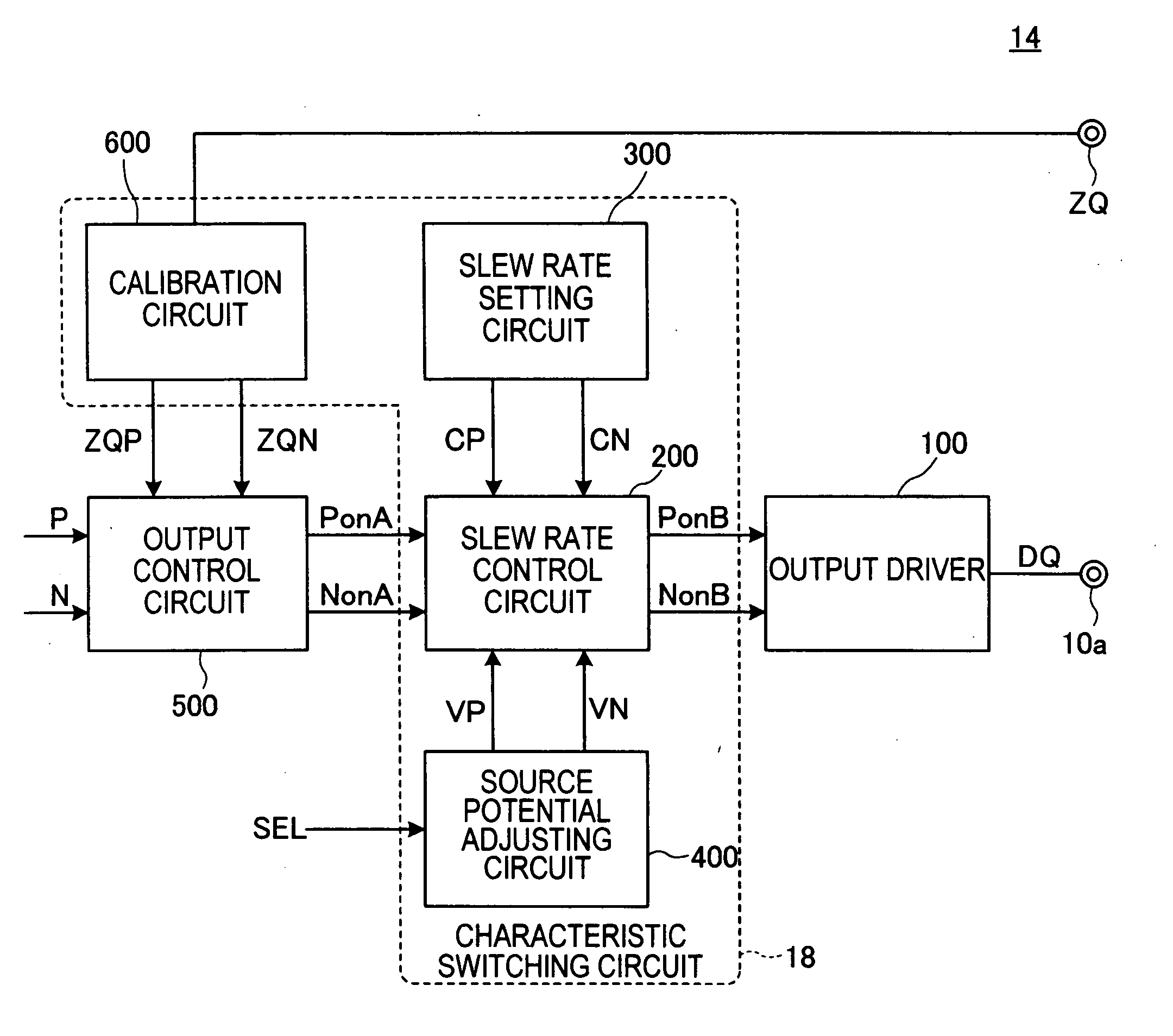
[0069]FIG. 7 is a block diagram of a configuration of the output circuit 14 according to the present invention.

[0070]As shown in FIG. 7, the output circuit 14 according to the first embodiment includes an output driver 100 that drives the data input and output terminal 10a, and a characteristic switching circuit 18 that switches characteristics of the output driver 100 based on the power voltage VDDQ. The characteristic switching circuit 18 includes a slew rate control circuit 200 that adjusts a slew rate of the output driver 100. Depending on ON signals NonB and PonB, the output driver 100 outputs a high level data DQ or a low level data DQ from the data input and output terminal 10a. Although it is not particularly limited thereto, in the first embodiment, both the ON signals NonB and PonB are 5-bit signals. This is because, as described later, a pull-up circuit PU and a pull-down circuit PD included in the output driver 100 are, respectively, constituted by five output transistor...

second embodiment

[0148]the present invention is explained next.

[0149]FIG. 25 is a block diagram of an output circuit 14a according to the second embodiment.

[0150]As shown in FIG. 25, the output circuit 14a according to the second embodiment differs from the output circuit 14 shown in FIG. 7 in that the switching signal SEL is also input into a calibration circuit 700 included in a characteristic switching circuit 18a. Because features of the output circuit 14a other than the above are identical to those of the output circuit 14 shown in FIG. 7, like elements are denoted by like reference numerals and redundant explanations thereof will be omitted.

[0151]FIG. 26 is a waveform diagram of the data DQ that is output from the output driver 100 according to the second embodiment. In FIG. 26, a waveform when the power voltage VDDQ is the first voltage VDDQ1 (1.5 V) and a waveform when the power voltage VDDQ is the second voltage VDDQ2 (1.25 V) are overlapped.

[0152]As shown in FIG. 26, the waveform when the ...


PUM


Abstract

The semiconductor device includes an output driver and a characteristic switching circuit that switches characteristics of the output driver. The characteristic switching circuit mutually matches a rising time and a falling time of an output signal output from the output driver, when a power voltage supplied to a power line is a first voltage, with a rising time and a falling time of the output signal output from the output driver, when the power voltage supplied to the power line is a second voltage. As a result, an increase in an influence of a harmonic component or a crosstalk when the power voltage is reduced does not occur. Moreover, because a receiving condition on a receiver side does not change even when the power voltage is reduced, signal transmission and reception can be performed correctly irrespective of the power voltage.

Description

BACKGROUND OF THE INVENTION[0001]1. Field of the Invention[0002]The present invention relates to a semiconductor device and an information processing system, and more particularly relates to a semiconductor device whose power voltage is variable and an information processing system including the same.[0003]2. Description of the Related Art[0004]In semiconductor devices such as DRAMs (Dynamic Random Access Memory), for standardization, a power voltage and the like is strictly determined by the standards. For example, in a DDR3 (Double Data Rate) SDRAM (Synchronous DRAM), the power voltage is defined to be 1.5 V (1 G bits DDR3 SDRAM (Document No. E1494E50 (Ver. 5.0)) <http: / / www.elpida.com / pdfs / E1494E50.pdf>).[0005]In recent years, because the demand for a low power consumption has been very high, many attempts have been made to reduce the power voltage. However, when the power voltage is changed, a waveform of an output signal output from an output driver also changes. Due to t...

Claims


Application Information

Patent Timeline
IPC IPC(8): H03K5/12
CPCH03K19/00384H03K19/00361
Inventor NISHIO, YOJI
Owner LONGITUDE LICENSING LTD
Why Eureka
Try Eureka