Cleaning method of apparatus for depositing carbon containing film

a technology of carbon containing film and cleaning method, which is applied in the direction of chemical vapor deposition coating, coating, chemical apparatus and processes, etc., can solve the problems of deterioration of the yield of a semiconductor device, and achieve the effect of a wide cleaning process margin and excellent reproducibility according to the reactor

Inactive Publication Date: 2011-05-19
WONIK IPS CO LTD
View PDF7 Cites 13 Cited by
  • Summary
  • Abstract
  • Description
  • Claims
  • Application Information

AI Technical Summary

Benefits of technology

[0010]As described above, the present invention provides an in-situ cleaning method of an apparatus for depositing a carbon-containing film. When, conventionally, cleaning is performed by using only a corrosive gas, a by-product in a solid form is generated in a reactor and thus, the reactor cannot be completely cleaned. In the present invention, the reactor can be cleaned without generating a by-product in a solid form by removing a metal by-product in the reactor by using a cleaning gas including halogens and adding a carbon-removing gas to the cleaning gas including halogens.
[0011]In particular, the present invention introduces a cleaning method of a reactor by partially activating gases. The cleaning gas is used in an activated state, and the carbon-removing gas is used without being activated. In the method, reproducibility according to reactors is excellent, and a wider cleaning process margin can be obtained.

Problems solved by technology

These particles cause defects in a deposition process and are attached to the wafer, which result in deterioration of the yield of a semiconductor device.

Method used


Image

  • Cleaning method of apparatus for depositing carbon containing film
  • Cleaning method of apparatus for depositing carbon containing film
  • Cleaning method of apparatus for depositing carbon containing film

Examples


embodiment 1

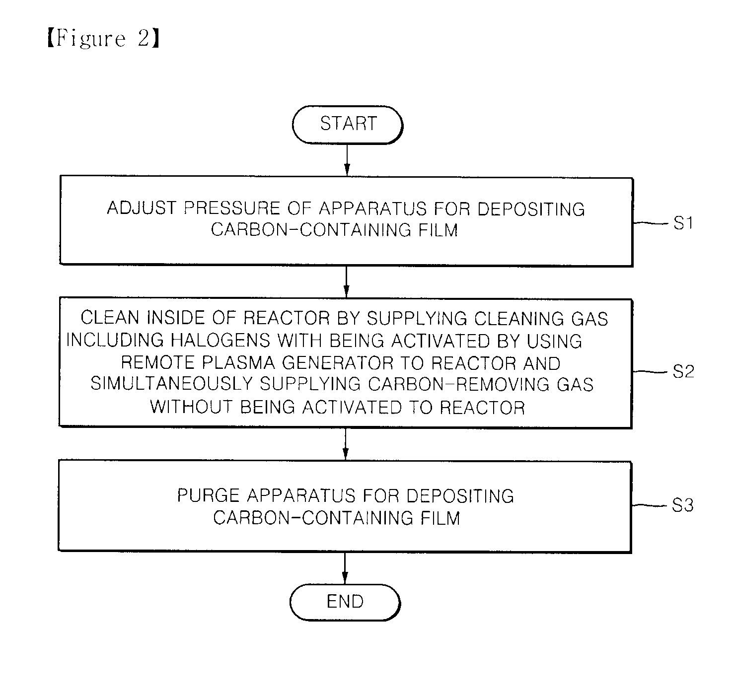
[0026]FIG. 2 is a flowchart illustrating a cleaning method according to an embodiment of the present invention.

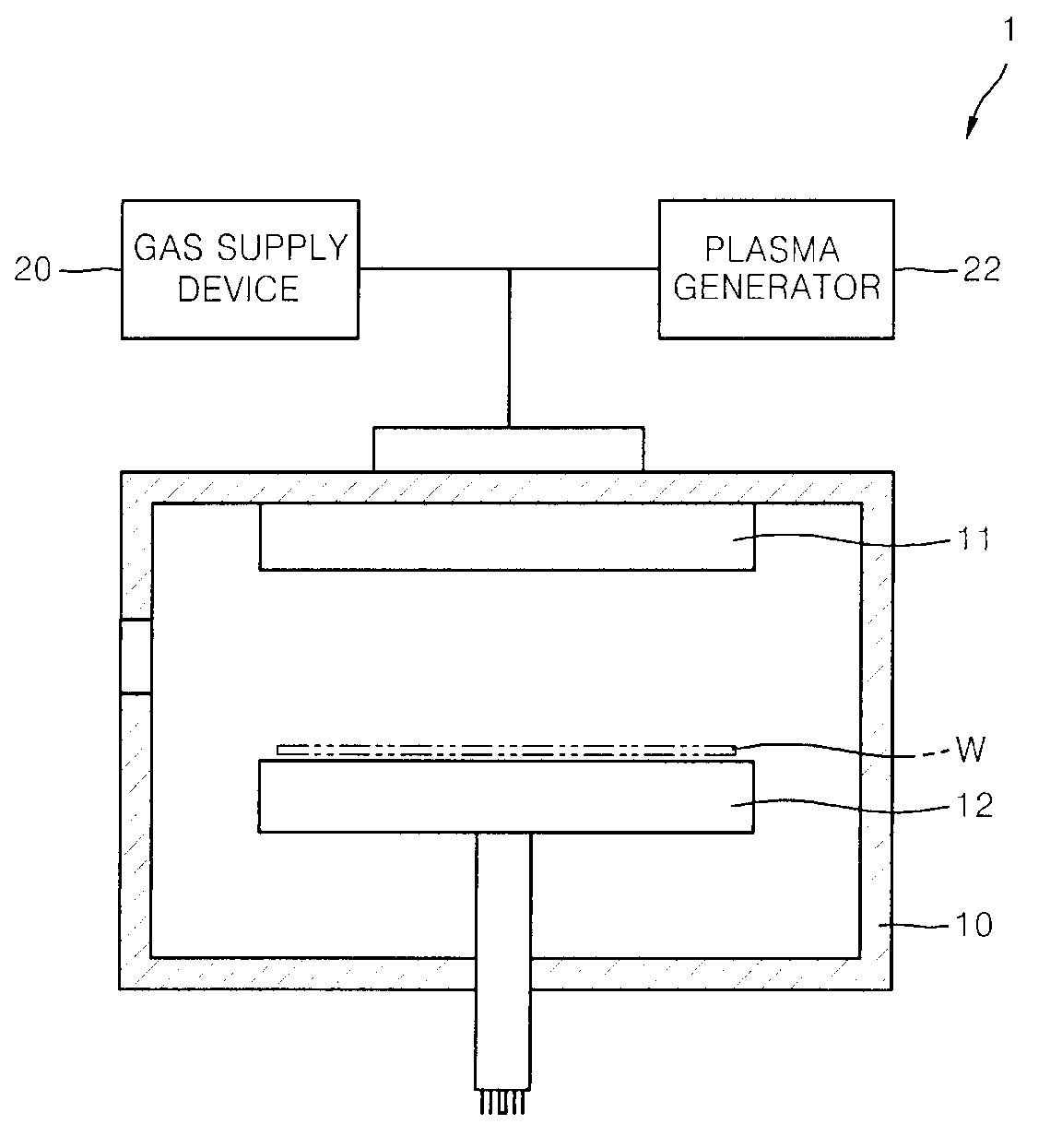
[0027]Referring to FIGS. 1 and 2, the pressure inside the reactor 10 of the apparatus 1 is adjusted to be suitable for cleaning, in operation s1 of FIG. 2. The pressure inside the reactor 10 is 0.3-10 torr. As the pressure inside the reactor 10 decreases, a cleaning efficiency increases. The pressure inside the reactor 10 is maintained at 0.5-4 torr.

[0028]Next, in operation s2, the inside of the reactor 10 is cleaned without stopping the apparatus 1 by supplying a cleaning gas including halogens with being activated by using a remote plasma generator 22 to the reactor 10 and simultaneously supplying a carbon-removing gas without being activated to the reactor 10. Time for the cleaning operation s2 varies according to the contamination degree of the reactor 10 and may vary depending on whether 1000 or 500 wafers are treated. Although changed according to conditions, carbon-c...

embodiment 2

[0033]FIG. 3 is a flowchart illustrating a cleaning method according to another embodiment of the present invention.

[0034]The cleaning method according to the present embodiment of the present invention is similar to the cleaning method of FIG. 2 but is different from the cleaning method of FIG. 2 in that additional operations are included.

[0035]Referring to FIGS. 1 and 3, the pressure inside the reactor 10 is adjusted to be suitable for cleaning, in operation s11 of FIG. 3.

[0036]Next, in operation s12, O2 treatment is performed. O2 treatment (s12) is performed to oxidize carbon on the surface of the by-product inside the reactor 10 and to primarily remove carbon.

[0037]Subsequently, in operation s13, the inside of the reactor 10 is cleaned by supplying a cleaning gas including halogens with being activated by using the remote plasma generator 22 to the reactor 10 and simultaneously supplying a carbon-removing gas without being activated to the reactor 10.

[0038]When the cleaning oper...


PUM

PropertyMeasurementUnit
pressureaaaaaaaaaa
pressureaaaaaaaaaa
resistanceaaaaaaaaaa

Abstract

A dry cleaning method of an apparatus for depositing a carbon-containing film is provided. The method includes in-situ cleaning an inside of a reactor of the apparatus, wherein the cleaning of the inside of the reactor of the apparatus comprises supplying a cleaning gas including halogens with being activated by using a remote plasma generator to the reactor and simultaneously supplying a carbon-removing gas without being activated to the reactor. In the method, a by-product in a solid form is not generated, and in-situ cleaning can be performed without stopping the apparatus for depositing a carbon-containing film after a predetermined amount of wafers are treated, such that productivity of the apparatus for depositing a carbon-containing film can be maximized.

Description

TECHNICAL FIELD [0001]The present invention relates to a cleaning method of an apparatus for manufacturing a semiconductor, and more particularly, to a dry cleaning method of a reactor of an apparatus for depositing a carbon-containing film.BACKGROUND ART [0002]Generally, semiconductor devices are manufactured by using a plurality of unit processes such as an ion implantation process, a film formation process, a diffusion process, a photolithography process, and an etching process. The film formation process among the unit processes is an essential process that must be improved in reproducibility and reliability of semiconductor device manufacturing.[0003]A film of a semiconductor device is formed on a wafer by using methods such as sputtering, evaporation, chemical vapor deposition (CVD), and atomic layer deposition (ALD) etc. Apparatuses for depositing a film used to perform the methods generally include a reactor, a gas line for supplying various kinds of gases to the reactor, an...

Claims


Application Information

Patent Timeline
Patent Type & Authority Applications(United States)
IPC IPC(8): B08B7/00
CPCC23C16/4405C23C16/4404
Inventor YOU, DONG-HOLEE, JUNG-WORK
Owner WONIK IPS CO LTD
Why Eureka
Try Eureka