

ZnO SEMICONDUCTOR ELEMENT
a technology of zno and semiconductor elements, which is applied in the direction of semiconductor devices, basic electric elements, electrical appliances, etc., can solve the problems of p-type zno not being obtained, degrading crystallinity, and no significant development of zno-based semiconductor as a semiconductor device material, so as to improve the properties and nature of the acceptor-doped layer, prevent the increase of crystal defects in the layer, and improve the flatness of the acceptor-
- Summary
- Abstract
- Description
- Claims
- Application Information
AI Technical Summary
Benefits of technology
Problems solved by technology
Method used
Image

Examples
Embodiment Construction
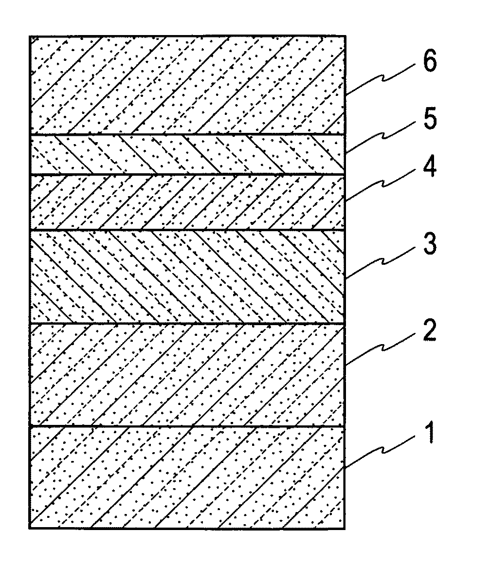
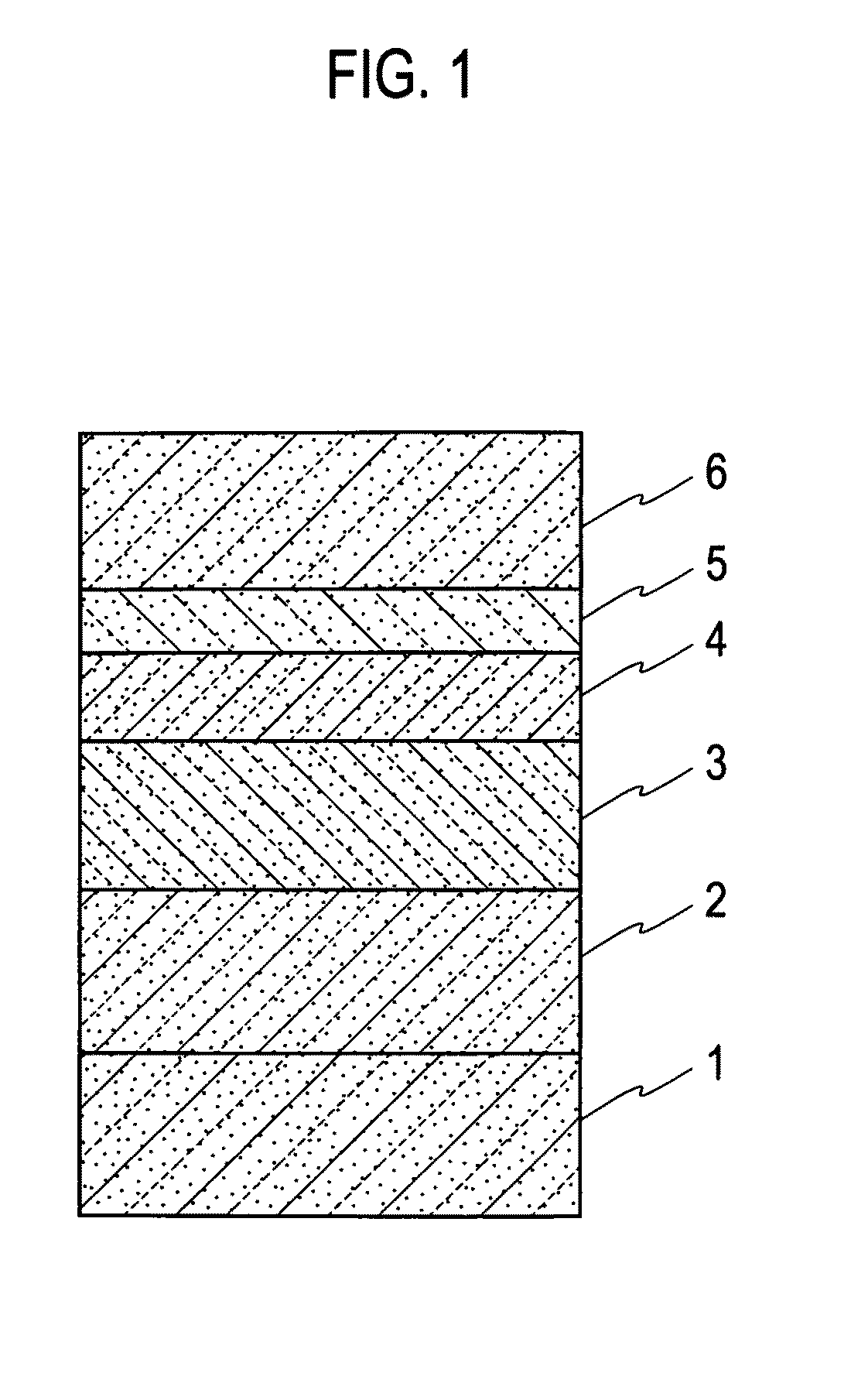
[0053]Hereinafter, an embodiment of the present invention will be described by referring to the drawings. The drawings are schematic, and thus differ from the actual. Additionally, some components may differ in dimensional relation and ratio in one drawing from the others. FIG. 1 shows an example of a laminate structure of a ZnO-based semiconductor device of the present invention.
[0054]On a ZnO substrate 1 serving as a substrate for growth, an n-type MgZZn1-ZO (0≦Z2, an undoped MgZnO layer 3, an MQW active layer 4, an undoped MgXZn1-XO (05, and an acceptor doped MgYZn1-YO (06 are sequentially laminated. Herein, in order to simplify the notations of the n-type MgZZn1-ZO layer 2, the undoped MgXZn1-XO layer 5, the acceptor-doped MgYZn1-YO layer 6, and the like, they are described as the n-type MgZZnO layer 2, the undoped MgXZnO layer 5, and the acceptor-doped MgYZnO layer 6, respectively. Hereinafter, the same applies to other notations.
[0055]Further, a ZnO-based semiconductor or a Zn...
PUM
 Abstract
Description
Claims
Application Information