Light emitting diode device

a technology of light-emitting diodes and led arrays, which is applied in the direction of semiconductor devices, basic electric elements, electrical appliances, etc., can solve the problems of less likely to achieve stable reliability, higher cost of manufacturing led array devices, and complicated led devices including led arrays. achieve the effect of reducing the light-absorption of metal electrodes, increasing the brightness, efficiency and service life of led devices

Active Publication Date: 2011-05-19
SEMILEDS OPTOELECTRONICS CO LTD
View PDF5 Cites 30 Cited by
  • Summary
  • Abstract
  • Description
  • Claims
  • Application Information

AI Technical Summary

Benefits of technology

[0014]The current spreading performance of a vertical LED device can be optimized and the light-absorption of a metal electrode can be reduced by applying an outwardly located metal electrode of the invention, thereby increasing the brightness, efficiency and service life of the LED device, and reducing energy costs.

Problems solved by technology

However, in terms of manufacturing, a LED device including a LED array is more complicated than a single LED device with high output power.
Therefore, the cost of manufacturing the LED array device is higher and the stable reliability is less likely to be achieved.
However, the semiconductor material layer used in a conventional LED usually has poor conductivity, such that electric current cannot be spread effectively and uniformly over an active layer from a contact.
Therefore, some areas inside the LED can produce high electric current density phenomenon, thereby affecting the whole brightness, even leading to early deterioration in the proximity of the active layer.
As a result, the service life of the LED is reduced significantly.
However, the increased thickness of the semiconductor material layer may not only increase production costs but also lead to stress problems.
Therefore, it is impossible to unlimitedly increase the thickness of the semiconductor material layer to comply with the current spreading performance requirement of a large-size LED device.
As a result, for the large-size device shown in FIG. 2, a satisfactory performance cannot be achieved merely by increasing the thickness of the semiconductor material layer.
It can be seen that the size of a LED is substantially limited by the current spreading characteristic of the semiconductor material layer.
However, most of the outlines of common LED devices are squares or rectangles, therefore it is difficult not only to place each radial metal wire on an emission layer such that the best current spreading performance can be achieved, but also to ensure that the adjacent radial metal wires have constant interval therebetween.
In addition, both sides of the metal electrode are high illumination sides, which tend to absorb emission light, thereby decreasing brightness.
Therefore, conventional LED devices still generally have the following problems including uneven current density, low light extraction efficiency, unsatisfactory brightness, unsatisfactory efficiency, short service life, and so on, which are to be solved.

Method used


Image

  • Light emitting diode device
  • Light emitting diode device
  • Light emitting diode device

Examples


Embodiment Construction

[0037]The preferred embodiments of the invention are described hereinafter, including various embodiments of vertical LED devices according to the invention, in which the current spreading performance of a semiconductor layer and the light-absorption property of a metal electrode have been modified, thereby achieving better brightness, efficiency and service life in comparison with conventional LED devices.

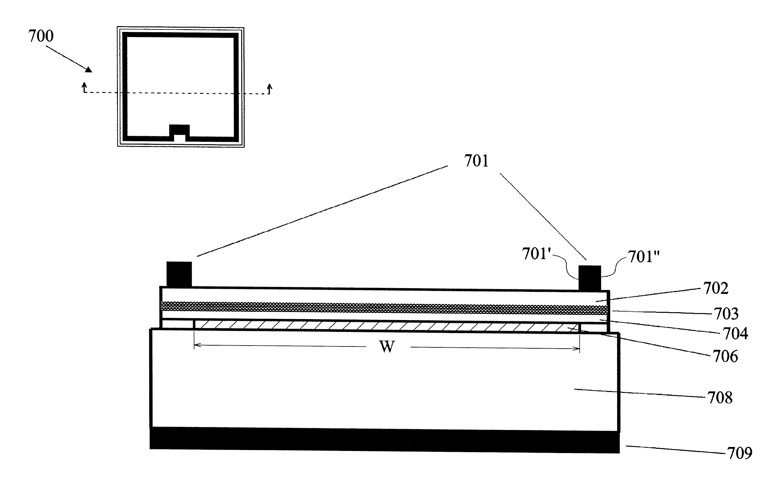
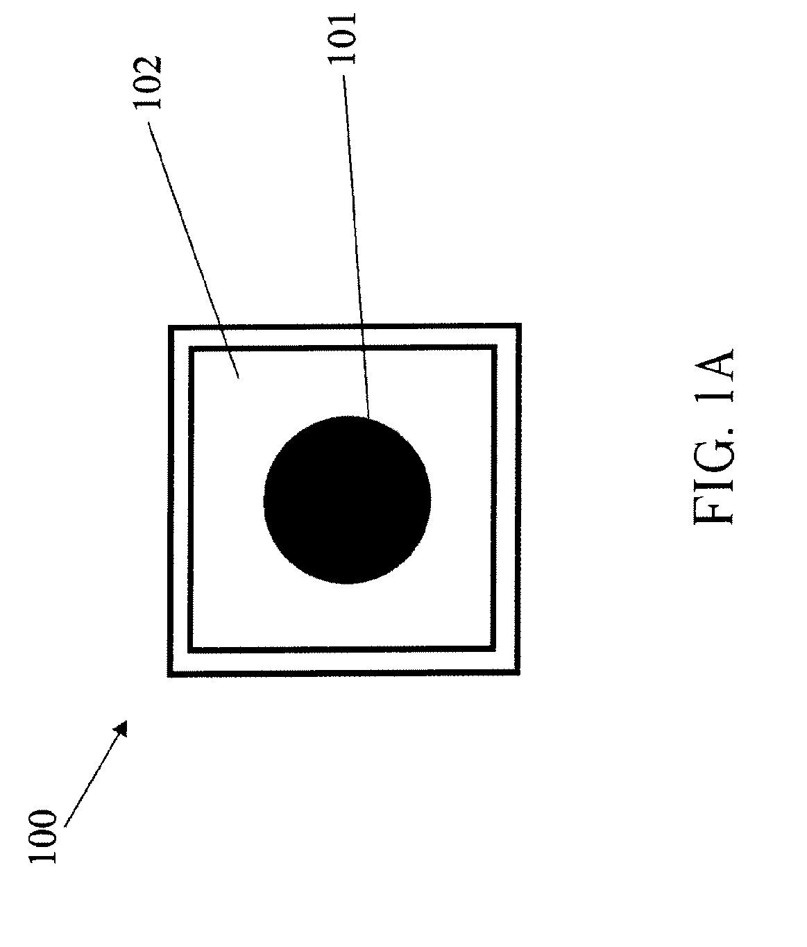
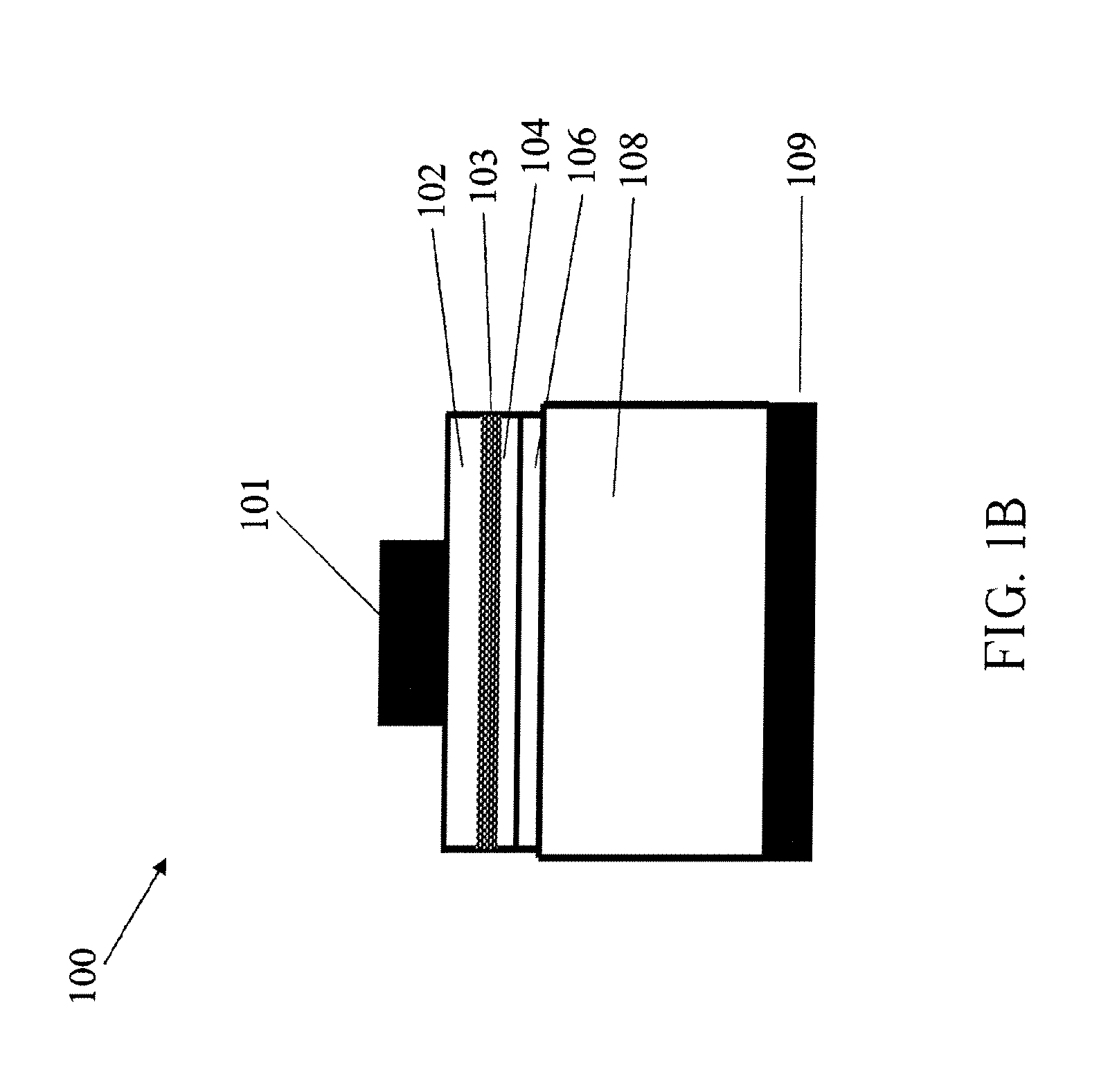
[0038]FIG. 4 shows a top view of a large-size vertical GaN-based (gallium nitride) LED device 300 according to one embodiment of the invention. FIG. 5 shows both of a top view and a cross-sectional view of the LED device 300 shown in FIG. 4. FIG. 6 illustrates a three dimensional view of the LED device 300 shown in FIG. 4. In this embodiment, the size of the n-type (second conductivity type) semiconductor layer 302 is 1 mm2. The large-size vertical LED device 300 of the invention includes a first electrode 309, a conductive base layer 308 formed on the first electrode 309, a refle...


PUM


Abstract

A high-brightness vertical light emitting diode (LED) device having an outwardly located metal electrode. The LED device is formed by: forming the metal electrode on an edge of a surface of a LED epitaxy structure using a deposition method, such as physical vapor deposition (PVD), chemical vapor deposition (CVD), evaporation, electro-plating, or any combination thereof; and then performing a packaging process. The composition of the LED may be a nitride, a phosphide or an arsenide. The LED of the invention has the following advantages: improving current spreading performance, reducing light-absorption of the metal electrode, increasing brightness, increasing efficiency, and thereby improving energy efficiency. The metal electrode is located on the edge of the device and on the light emitting side. The metal electrode has two side walls, among which one side wall can receive more emission light from the device in comparison with the other one.

Description

CLAIM OF PRIORITY[0001]This application claims the priority benefit of Taiwan Application Serial Number 98137664, filed on Nov. 6, 2009. All disclosure of the Taiwan application is incorporated herein by reference.BACKGROUND OF THE INVENTION[0002]A. Field of the Invention[0003]The present invention is directed to a vertical light emitting diode (LED) device, and more particularly to a high-brightness LED device having an outwardly located metal electrode.[0004]B. Description of the Prior Art[0005]Currently, LED is widely applied in our daily life due to its characteristics of low production cost, easy fabrication, small size, low power consumption and high efficiency, for example, in the fields of cell phones, electric boards, electric torches, traffic lights and so on. Nevertheless, improvements in the luminous efficiency and brightness of a LED are pursued continuously.[0006]Recently, high-brightness LEDs using nitrides and phosphides have been developed, which can not only emit r...

Claims


Application Information

Patent Timeline
Patent Type & Authority Applications(United States)
IPC IPC(8): H01L33/32H01L33/60
CPCH01L33/22H01L33/405H01L33/60H01L33/38H01L33/36H01L33/46
Inventor LIU, WEN-HUANGSHAN, LI-WEICHU, CHEN-FU
Owner SEMILEDS OPTOELECTRONICS CO LTD
Why Eureka
Try Eureka