Method of Producing a Surface Plasmon Generator, a Surface Plasmon Generator and a Sensor Incorporating the Surface Plasmon Generator

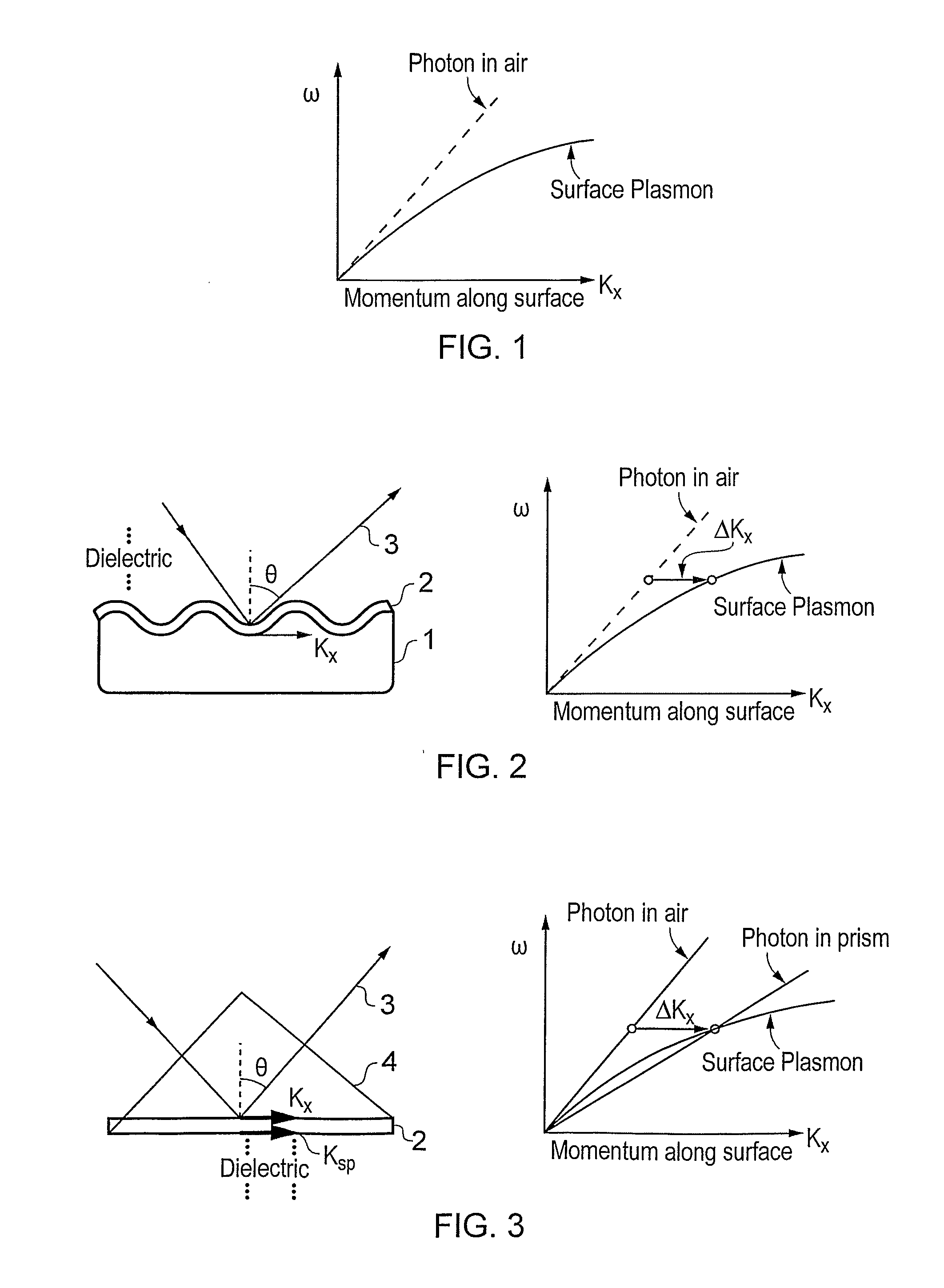
a surface plasmon and generator technology, applied in the field of surface plasmon generation, can solve the problems of in-prism reflected light loss, two cannot couple or “transform” between each other, and require bulky and cumbersome prisms, so as to reduce the space required by the surface plasmon generator, reduce stress, and enhance penetration of guided electromagnetic energy.

Inactive Publication Date: 2011-05-19
ASTON UNIV
View PDF13 Cites 11 Cited by
  • Summary
  • Abstract
  • Description
  • Claims
  • Application Information

AI Technical Summary

Benefits of technology

The benefit of employing materials supporting a relatively large skin depth is to enhance penetration of guided electromagnetic energy to the surfaces arranged to support surface plasmons in the surface plasmon generator.
The optical waveguide may be maintained in an un-flexed state, at least in the proximity of the layer or second optical waveguide thereby reducing the space required by the surface plasmon generator, reducing stresses. The optical waveguide may possess optical waveguide cladding but is preferably otherwise not itself embedded, or encased in any holding substrate of material (such as epoxy), thus, the outer circumferential surface / length of the optical waveguide may be exposed.
The optical waveguide may have a core part and a cladding part adjacent to the core part which is lapped to define a proximal outer surface area being closer to the core part than are other adjacent outer surface areas of the cladding part. The proximal outer surface area may, but preferably does not, expose a part of the waveguide core. The lapped cladding part enables not only the formation of a flat interface and outwardly presented (e.g. exposed) outer layer of material(s) or second optical waveguide surface, but also enables greater proximity of the interface between the layer of material(s), or second optical waveguide, to the core part of the optical waveguide from which surface plasmon inducing radiative modes derive. The lapped region of the waveguide may be such as to present a D-shaped cross-sectional profile if viewed in a direction along the waveguide (e.g. fibre) axis, the proximal outer surface area defining the flat part of the D. The thickness of cladding at the lapped cladding part is preferably between about 15 μm and 5 μm, though other optimal thicknesses may be employed.

Problems solved by technology

Consequently, the two cannot couple or “transform” between each other due to being unable to satisfy the requirements of both energy and momentum conservation during “transformation”.
However, these prior art surface plasmon generating arrangements, and sample sensing methodologies, either require plasmon-exciting light to first pass through the dielectric sample (εd) being sensed (e.g. surface grating arrangements), or require bulky and cumbersome prisms (the Kretschmann arrangement) which also suffer from in-prism reflected light losses due to reflection at prism surfaces.
Both of the above techniques fundamentally rely upon monitoring changes in the intensity of reflected plasmon-exciting light and so suffer the detrimental consequences of irregularities or impurities at the light-reflecting (prism or grating) surface.

Method used


Image

  • Method of Producing a Surface Plasmon Generator, a Surface Plasmon Generator and a Sensor Incorporating the Surface Plasmon Generator
  • Method of Producing a Surface Plasmon Generator, a Surface Plasmon Generator and a Sensor Incorporating the Surface Plasmon Generator
  • Method of Producing a Surface Plasmon Generator, a Surface Plasmon Generator and a Sensor Incorporating the Surface Plasmon Generator

Examples


Embodiment Construction

; FURTHER OPTIONS AND PREFERENCES

System Overview

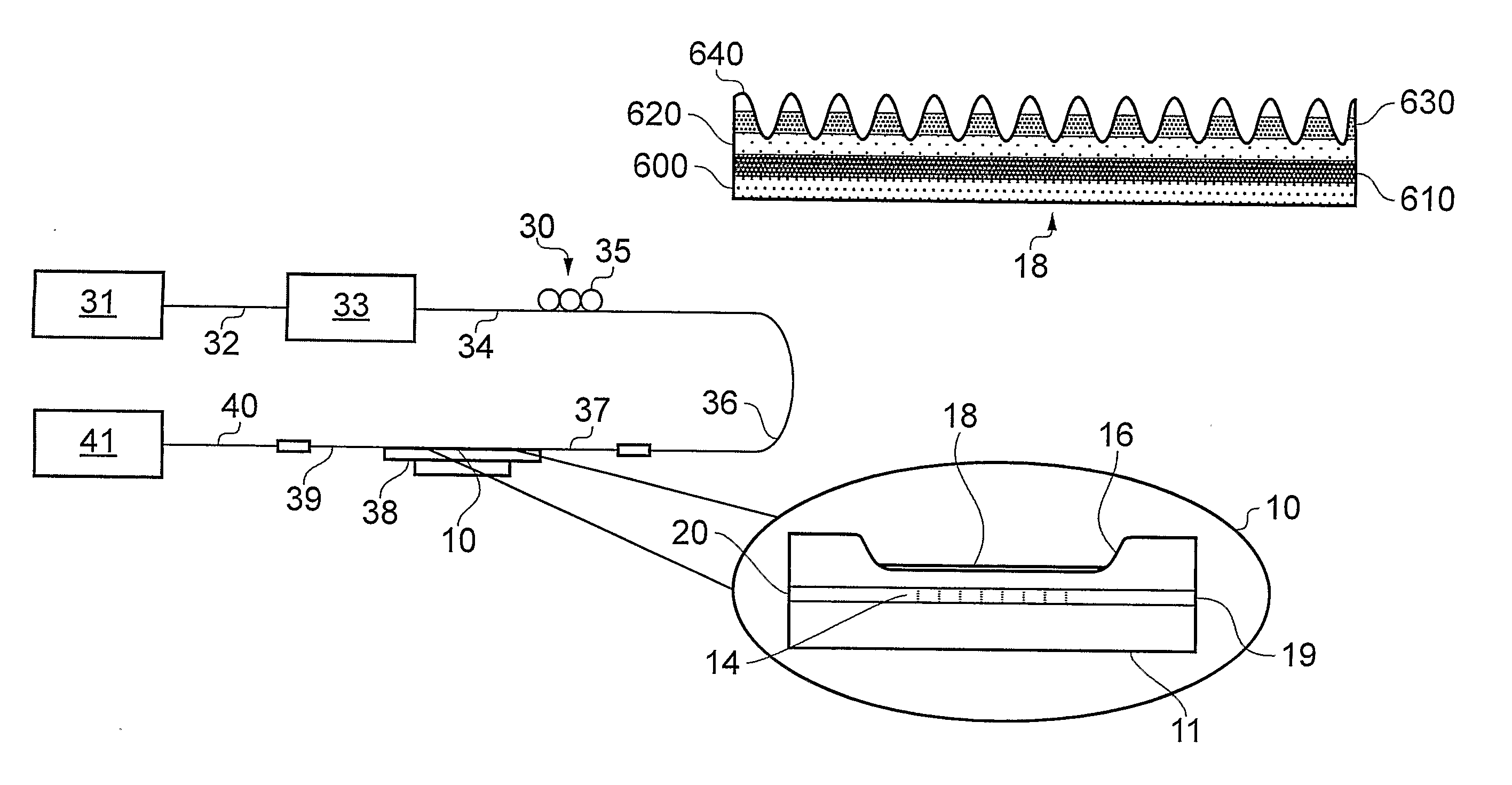
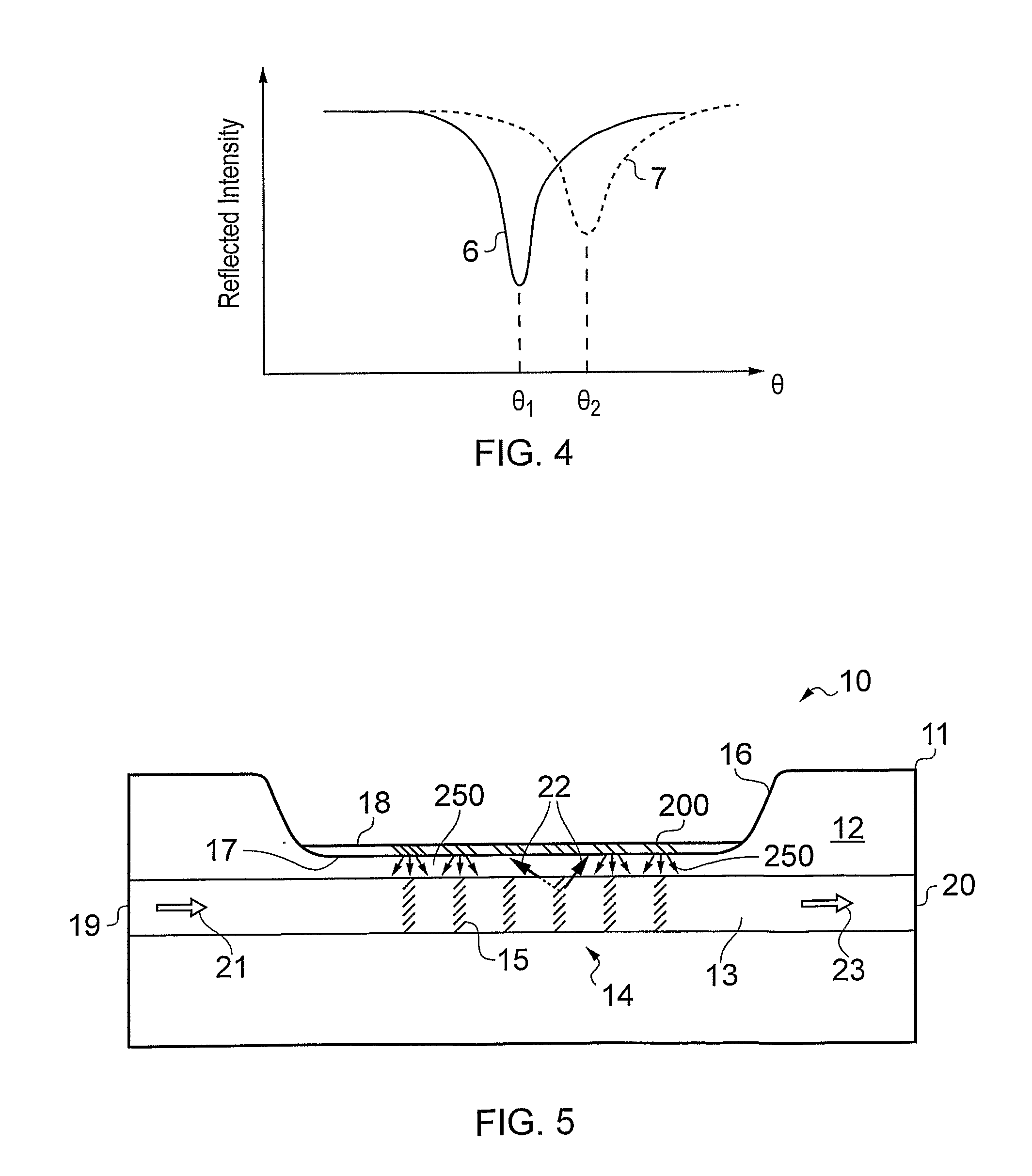
Referring to FIG. 5 there is schematically illustrated, in cross section, an example of a surface plasmon generator 10 according to an example of the present invention.

The surface plasmon generator includes a length of optical fibre 11 having an optical signal input part 19 comprising an open end of the optical fibre length arranged for receiving optical signals into the optical fibre, and an optical output part 20 comprising an open end of the optical fibre from which output optical signals can be received from the optical fibre.

The optical fibre has an optical fibre core part 13 clad by an optical fibre cladding 12. The diameter of the core part, and the dimensions, structure and design of the optical fibre as a whole, are such as to render the optical fibre a single-mode optical fibre in respect of optical signals having a wavelength in excess of about 1000 nanometres (as measured in vacuum).

The cladding part of the optical fibre is...


PUM

PropertyMeasurementUnit
refractive indexaaaaaaaaaa
wavelengthsaaaaaaaaaa
skin depthaaaaaaaaaa

Abstract

Surface plasmon generation on a metal or semiconductor layer at an outer surface of an optical waveguide, using light reflected or scattered from inside the optical waveguide. One aspect provides a main optical waveguide (11) (e.g. optical fibre) having a second optical waveguide (18) adhered thereto, the second optical waveguide including an optically transparent material (610) separating two surface plasmon supporting layers (600, 620). Another aspect provides a surface plasmon supporting layer of material(s) adhered to the main optical waveguide, the layer having photo-induced regions of material compaction. The regions of compaction may cause un-inscribed refractive index modulations in the main optical waveguide. The surface plasmons are coupled to the guided mode(s) in the main optical waveguide. Surface plasmon resonance depends on sample material in contact with an outermost surface plasmon supporting layer. Properties of the sample material can thus be detected in output guided mode(s) because of the coupling with the generated surface plasmons.

Description

FIELD OF THE INVENTIONThe present invention relates to the generation of surface plasmons, and particularly, though not exclusively, to sensing methods and apparatus using surface plasmons.BACKGROUND TO THE INVENTIONFree electrons of a metal can be treated as an electron liquid of high density. At the surface of a metal or semiconductor, longitudinal electron density fluctuations, or plasma oscillations, may occur and will propagate along the surface.These coherent fluctuations are accompanied by an electromagnetic field comprising a component transverse to (i.e. away from) the surface, and a component(s) parallel to the surface. The transverse electromagnetic field falls rapidly with increasing distance from the metal or semiconductor surface, having its maximum at the surface, and is sensitive to the properties of the metal or semiconductor surface and the properties of the dielectric substance (e.g. air, aqueous solution) immediately at and above the surface and into which the tr...

Claims


Application Information

Patent Timeline
Patent Type & Authority Applications(United States)
IPC IPC(8): G01N21/55G02F1/295G02B1/12
CPCB82Y20/00G01N21/553G02B6/1226G01N2021/258G01N21/7743
Inventor ALLSOP, THOMAS DAVID PAULBENNION, IANWEBB, DAVID JOHNNEAL, RONALD
Owner ASTON UNIV
Why Eureka
Try Eureka