Semiconductor device and driving method thereof

a technology of semiconductor devices and drives, applied in semiconductor devices, digital storage, instruments, etc., can solve the problems of short data holding time, difficult to sufficiently reduce power consumption, and loss of stored data, so as to achieve the effect of reducing power consumption, storing data for an extremely long time, and avoiding data loss

Inactive Publication Date: 2011-05-19
SEMICON ENERGY LAB CO LTD
View PDF23 Cites 50 Cited by
  • Summary
  • Abstract
  • Description
  • Claims
  • Application Information

AI Technical Summary

Benefits of technology

[0012]An object of one embodiment of the present invention is to provide a semiconductor device in which the adverse effect of variation on the threshold voltage of the transistor is suppressed and a plurality of states (e.g., states of three or more) are distinguished clearly and easily.
[0014]One embodiment of the present invention is a semiconductor device including a circuit which selects a voltage for correction on the basis of a comparison result between the potential of a bit line and a potential which is read out such that a plurality of states (e.g., states of three or more) are distinguished clearly and easily.
[0031]Since the off-state current of a transistor using an oxide semiconductor is extremely low, stored data can be held for an extremely long time by using the transistor. In other words, power consumption can be adequately reduced because refresh operation becomes unnecessary or the frequency of refresh operation can be extremely low. Moreover, stored data can be held for a long time even when power is not supplied.
[0032]Further, data can be written without high voltage, and deterioration of the element is not caused. Furthermore, since data is written depending on the on / off state of the transistor, high-speed operation can be easily realized. In addition, there is no need of operation for erasing data.
[0033]Further, since a transistor using a material other than an oxide semiconductor can operate at higher speed than a transistor using an oxide semiconductor, stored data can be read out at high speed by using the transistor.
[0034]According to one embodiment of the present invention, a voltage for correction is selected on the basis of the comparison result between the potential of the bit line and the potential read out, so that a plurality of states (for example, states of three or more) can be distinguished accurately and easily. Accordingly, a multi-valued type semiconductor device with excellent characteristics can be provided.

Problems solved by technology

Moreover, the transistor included in the storage element has a leakage current and electric charge flows into or out of the capacitor even when the transistor is not selected, so that the data holding time is short.
For that reason, writing operation (refresh operation) is necessary at predetermined intervals, and it is difficult to sufficiently reduce power consumption.
Furthermore, since stored data is lost when power supply stops, another storage device using a magnetic material or an optical material is further needed in order to hold data for a long time.
However, cost per storage capacitance is high because the circuit such as a flip-flop is used.
Moreover, as in a DRAM, stored data in an SRAM is lost when power supply stops.
However, a gate insulating layer included in a storage element deteriorates due to tunneling current generated in writing data, so that the storage element stops its function after a predetermined frequency of writing data.
However, this method involves a complicated peripheral circuit.
Moreover, employing such a method does not solve the fundamental problem of lifetime.
In other words, a flash memory is not suitable for applications in which data is frequently rewritten.
Further, it takes a relatively long time to hold or remove electric charge, and it is not easy to perform writing or erasing data at higher speed.
Further, a so-called multi-valued memory which holds a plurality of states in one storage element involves a complicated circuit in order to secure the accuracy of the writing, which causes reduction in the operation speed.

Method used


Image

  • Semiconductor device and driving method thereof
  • Semiconductor device and driving method thereof
  • Semiconductor device and driving method thereof

Examples


embodiment 1

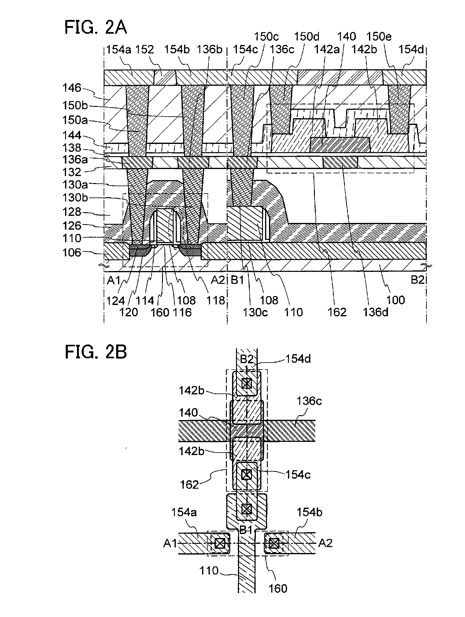
[0062]In Embodiment 1, structures and a manufacturing method of a semiconductor device according to one embodiment of the present invention will be described with reference to FIG. 1, FIGS. 2A and 2B, FIGS. 3A to 3H, FIGS. 4A to 4G, FIGS. 5A to 5D, FIG. 6, FIGS. 7A and 7B, FIGS. 8A and 8B, FIG. 9, FIG. 10, FIGS. 11A and 11B, FIGS. 12A and 12B, and FIGS. 13A and 13B.

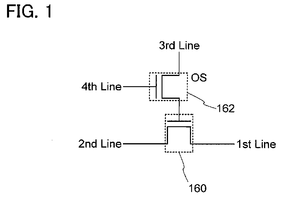
[0063]FIG. 1 illustrates an example of a circuit configuration of a semiconductor device. The semiconductor device includes a transistor 160 using a material other than an oxide semiconductor, and a transistor 162 using an oxide semiconductor. In FIG. 1, reference symbol OS is denoted for clear description of an oxide semiconductor which is used for the transistor 162.

[0064]A gate electrode of the transistor 160 is electrically connected to one of a source electrode or a drain electrode of the transistor 162. A first wiring (a 1st line, also referred to as a source line) is electrically connected to a source electrode of ...

modification example

[0184]FIG. 10, FIGS. 11A and 11B, FIGS. 12A and 12B, and FIGS. 13A and 13B illustrate modification examples of a structure of a semiconductor device. The semiconductor devices in each of which the transistor 162 has a structure different from that described above will be described below as modification examples. That is, the structure of the transistor 160 is the same as the above.

[0185]FIG. 10 illustrates an example of a semiconductor device including the transistor 162 in which the gate electrode 136d is placed below the oxide semiconductor layer 140 and the source and drain electrodes 142a and 142b are in contact with a bottom surface of the oxide semiconductor layer 140. Note that the planar structure can be changed as appropriate to correspond to the cross section; therefore, only the cross section is shown here.

[0186]A big difference between the structure in FIG. 10 and the structure in FIG. 2A is the position at which the oxide semiconductor layer 140 is connected to the sour...

embodiment 2

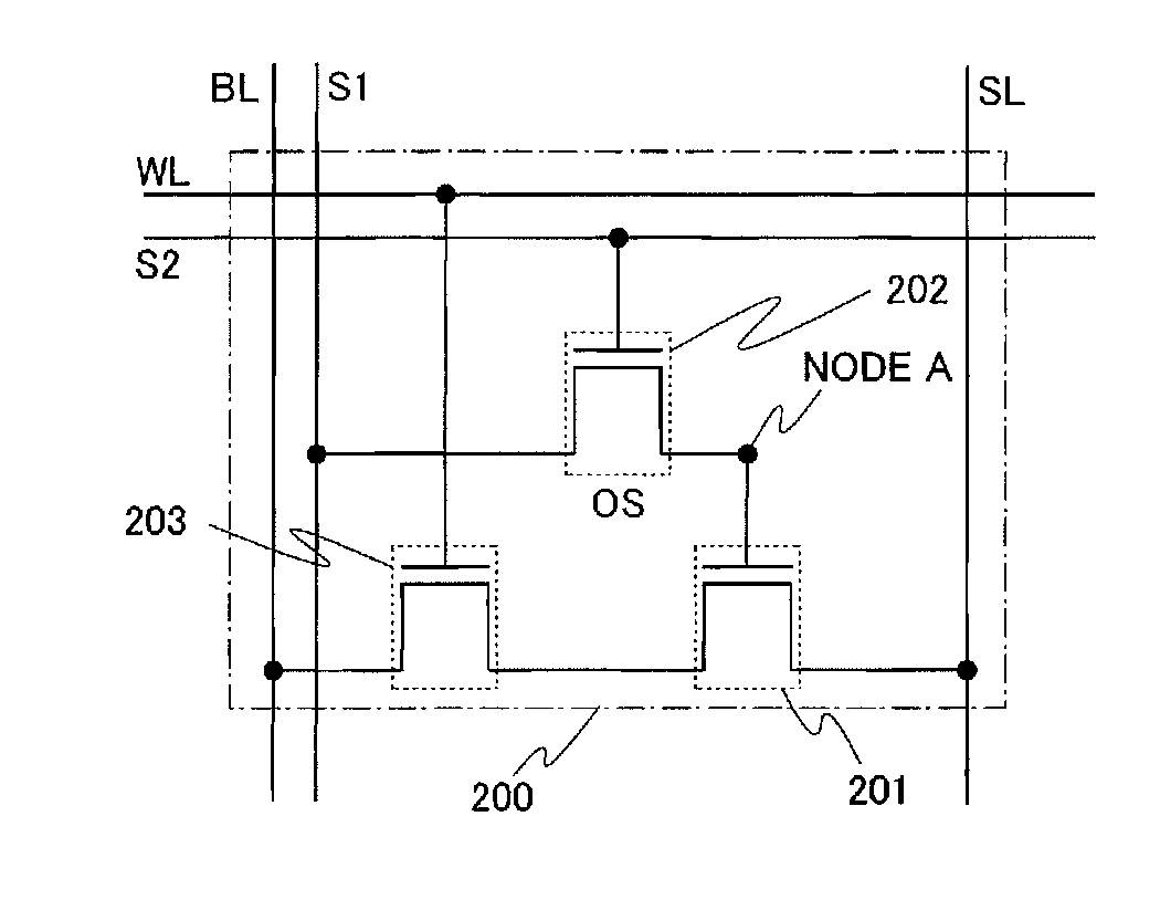
[0212]In Embodiment 2, a circuit configuration and operation of a semiconductor device according to one embodiment of the present invention will be described.

[0213]FIG. 14 illustrates an example of a circuit diagram of a semiconductor device (hereinafter also referred to as a memory cell). A memory cell 200 shown in FIG. 14 includes a source line SL, a bit line BL, a first signal line S1, a second signal line S2, a word line WL, a transistor 201, a transistor 202, and a transistor 203. The transistors 201 and 203 are formed using a material other than an oxide semiconductor; the transistor 202 is formed using an oxide semiconductor.

[0214]A gate electrode of the transistor 201 and one of a source electrode and a drain electrode of the transistor 202 are electrically connected to each other. The source line SL is electrically connected to a source electrode of the transistor 201, and a drain electrode of the transistor 201 is electrically connected to a source electrode of the transis...


PUM


Abstract

A semiconductor device includes: a source line; a bit line; a word line; a memory cell connected to the bit line and the word line; a driver circuit which drives a plurality of second signal lines and a plurality of word lines so as to select the memory cell specified by an address signal; a potential generating circuit which generates a writing potential and a plurality of reading potentials to supply to a writing circuit and a reading circuit; and a control circuit which selects one of a plurality of voltages for correction on a basis of results of the reading circuit comparing a potential of the bit line with the plurality of reading potentials.

Description

TECHNICAL FIELD[0001]The present invention relates to a semiconductor device using a semiconductor element, a method for manufacturing the semiconductor device, and a method for driving the semiconductor device.BACKGROUND ART[0002]Storage devices using semiconductor elements are broadly classified into two categories: a volatile storage device that loses stored data when power supply stops, and a non-volatile storage device that holds stored data even when power supply stops.[0003]A typical example of a volatile storage device is a DRAM (dynamic random access memory). A typical example of a volatile storage device is a DRAM (dynamic random access memory). A DRAM stores data in such a manner that a transistor included in a storage element is selected and electric charge is stored in a capacitor.[0004]Electric charge in the capacitor is lost by reading data from DRAM on the above-described principle; thus, writing operation is necessary every time data is read out. Moreover, the trans...

Claims


Application Information

Patent Timeline
Patent Type & Authority Applications(United States)
IPC IPC(8): G11C11/4096
CPCG11C7/062H01L29/205G11C2207/005H01L21/02554H01L21/02565H01L21/02631H01L27/0688H01L27/105H01L27/11519H01L27/11521H01L27/11524H01L27/11551H01L27/1156H01L27/1203H01L27/1225H01L29/155G11C7/067H10B41/10H10B41/20H10B41/30H10B41/35H10B41/70G11C11/40
Inventor YAMAZAKI, SHUNPEIKOYAMA, JUNKATO, KIYOSHI
Owner SEMICON ENERGY LAB CO LTD
Why Eureka
Try Eureka