Synchronising between clock domains

a clock domain and clock domain technology, applied in the field of data processing systems, can solve the problems of difficult switching between the use of these mechanisms, and change can take many hundreds of processing cycles to perform, and achieve the effect of reducing hardware overhead and increasing synchronisation delay

Active Publication Date: 2011-05-19
ARM LTD
View PDF4 Cites 31 Cited by
  • Summary
  • Abstract
  • Description
  • Claims
  • Application Information

AI Technical Summary

Benefits of technology

[0027]The transition register used to hold the pre-switch pointer value during the change of synchronisation path may be advantageously provided by reuse of a latch which is included in another synchronising path not taking part in the switch being performed. This reduces the hardware overhead of the present technique.
[0028]Control of the transition register may be conveniently performed by a control delay path formed of serially connected latches matching the serially connected latches forming one of the plurality of synchronising paths. The synchronising path which is matched may be the longest synchronising path and typically the one which when switched into use produces an increase in synchronisation delay. Accordingly, forming the control delay path matched to this longest synchronising delay has the result that if, depending upon the process or implementation being used, the longest synchronising delay is altered, then the control delay path may readily be altered in the same way in order that correct operation of the circuit be maintained.

Problems solved by technology

While it is possible to use synchronisation mechanisms which deal with these synchronisation challenges individually, it is difficult to switch between the use of these mechanisms.
Such a change can take many hundreds of processing cycles to perform and this is a significant disadvantage.

Method used


Image

  • Synchronising between clock domains
  • Synchronising between clock domains
  • Synchronising between clock domains

Examples


Embodiment Construction

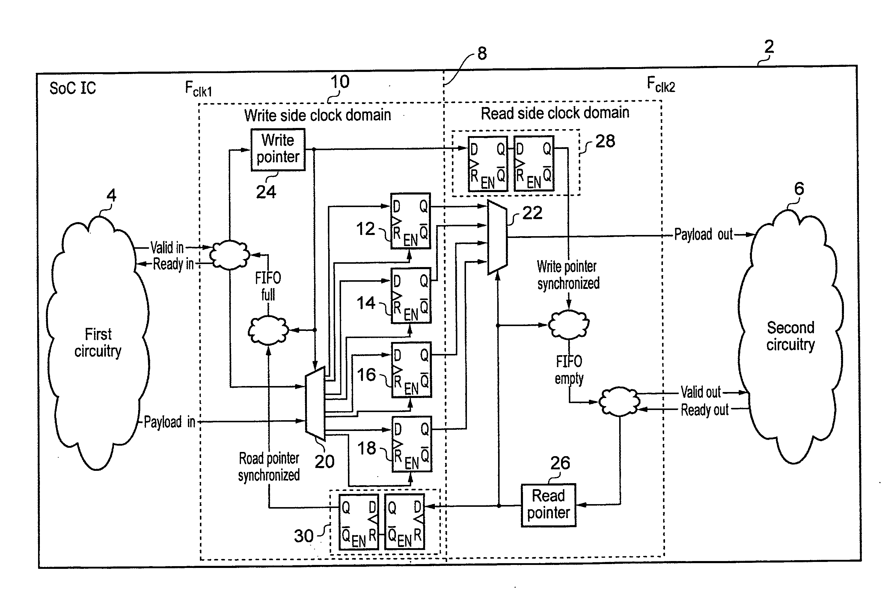
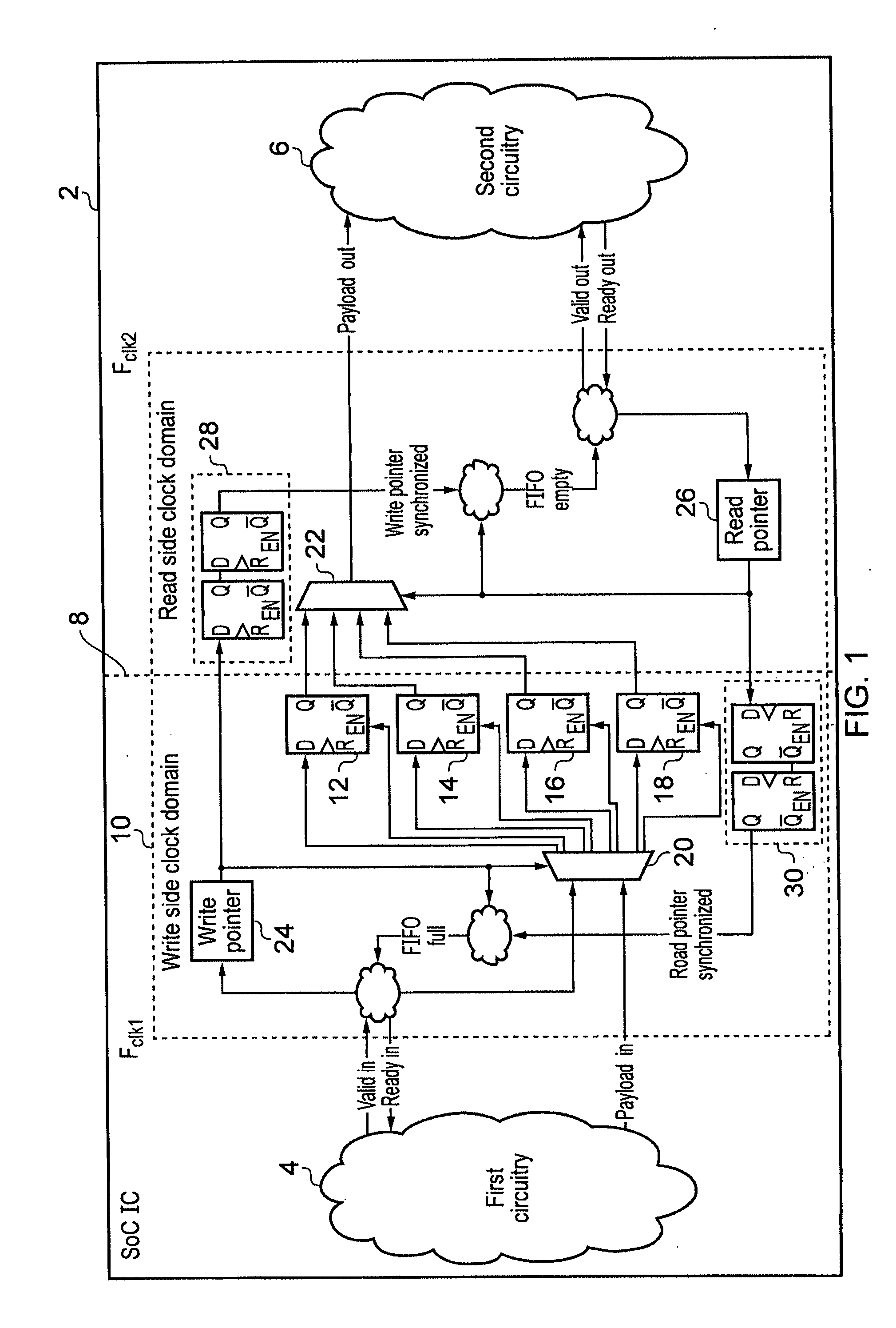
[0053]FIG. 1 illustrates a system-on-chip integrated circuit 2 including first circuitry 4 located within a first clock domain and second circuitry 6 located within a second clock domain. In this example embodiment the first circuitry 4 is arranged to pass a data value (payload) across a clock boundary 8 to the second circuitry 6. Accordingly, the first circuitry 4 is on the write side and the second circuitry 6 is on the read side of a first-in-first-out memory (FIFO) 10. This FIFO 10 has four memory slots 12, 14, 16, 18 which are written to by the first circuitry via a de-multiplexer 20. On the read side, the second circuitry 6 reads these memory slots 12, 14, 16, 18 via a multiplexer 22. A write pointer controls the selection made by the de-multiplexer 20 of the next memory slot 12, 14, 16, 18 to be written to and a read pointer controls the multiplexer 22 to point to the next memory slot 12, 14, 16, 18 from which a data value is to be read. The write pointer is stored within the...


PUM


Abstract

An integrated circuit 2 is provided with multiple clock domains separated by a clock boundary 8. Data values are passed across the clock boundary 8 using a first-in-first-out memory (FIFO), a read pointer and a write pointer for the FIFO are passed across the clock boundary 8 and must be synchronised to the receiving clock frequency. The clocks being used on either side of the clock boundary 8 may be switched and have a variable relationship therebetween. Multiple synchronisation paths are provided within pointer synchronising circuitry 32 which are used depending upon the particular relationship between the clocks on either side of the clock boundary 8. A pre-switch pointer value is held in a transition register 44 until a post-switch pointer value is available from the new synchronising path 36 when a switch in clock mode is made which requires an increase in synchronisation delay.

Description

BACKGROUND OF THE INVENTION[0001]1. Field of the Invention[0002]This invention relates to the field of data processing systems. More particularly, this invention relates to the field of synchronising between clock domains within data processing systems.[0003]2. Description of the Prior Art[0004]It is known to provide data processing systems having multiple clock domains. As an example, one clock domain may operate at a high frequency to perform computationally intensive tasks while another clock domain operates at a lower clock frequency to perform less demanding tasks. In order that these two clock domains can communicate, it is necessary to provide synchronisation mechanisms for passing signals between the domains. One known way of doing this is to utilise a first-in-first-out memory (FIFO) between the two clock domains with data values being written into the FIFO from one clock domain and then read out of the FIFO from another clock domain. In order that the writing and reading o...

Claims


Application Information

Patent Timeline
Patent Type & Authority Applications(United States)
IPC IPC(8): G11C8/18
CPCG06F5/10H03K5/135G06F2205/106
Inventor HAY, TIMOTHY NICHOLASFEERO, BRETT STANLEY
Owner ARM LTD
Why Eureka
Try Eureka