Organic electroluminescence display apparatus

a technology of electroluminescence display and electroluminescence, which is applied in the direction of electric variable regulation, process and machine control, instruments, etc., can solve the problem that the voltage applied between the source and the drain of the switching tft exceeds the withstand voltage, and achieves the effect of reducing the withstand voltage, simplifying the process, and reducing the cos

Inactive Publication Date: 2011-05-26
CANON KK
View PDF7 Cites 16 Cited by
  • Summary
  • Abstract
  • Description
  • Claims
  • Application Information

AI Technical Summary

Benefits of technology

[0014]Thereby, at least one light-emitting device among the stacked light-emitting devices is nonemission-treated, so that a data signal voltage to be supplied to one subpixel can be decreased. Therefore, the organic electroluminescence display apparatus can lower the withstand voltage between the source and the drain required for the switching TFT, and can be formed to be the active matrix type.
[0015]In addition, the or

Problems solved by technology

Therefore, when the structure in the above described document is formed to be the active matrix type, the structure causes

Method used


Image

  • Organic electroluminescence display apparatus
  • Organic electroluminescence display apparatus
  • Organic electroluminescence display apparatus

Examples


example 1

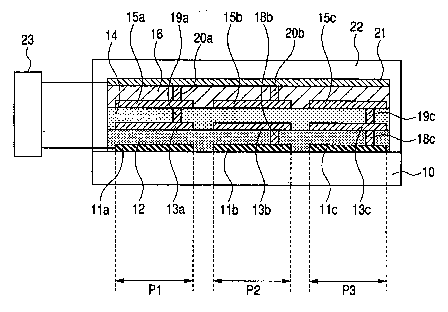
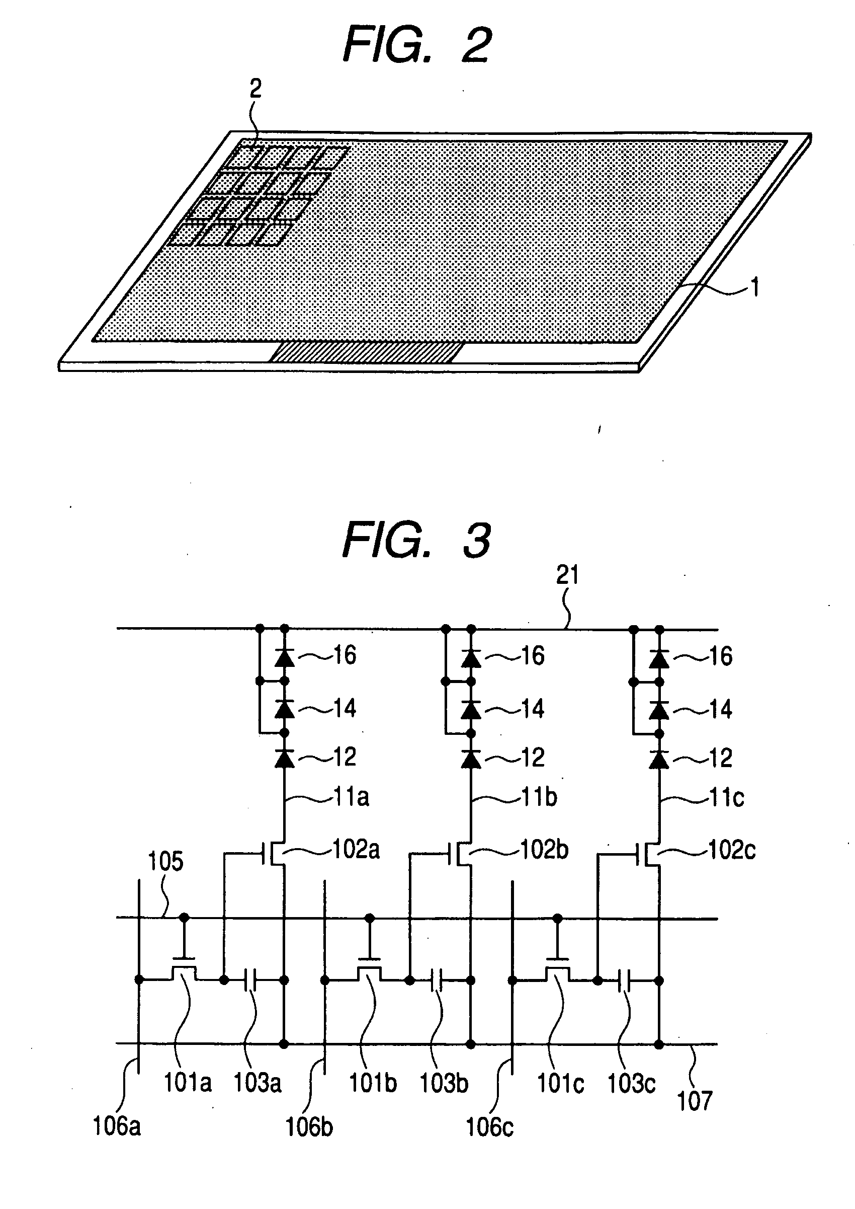
[0027]FIG. 1 is a view schematically illustrating a sectional structure in one pixel region of an organic electroluminescence display apparatus according to the present invention. A plurality of pixels 2 having the sectional, structure illustrated in FIG. 1 is arranged in a matrix form, and constitute a display region 1 of the organic electroluminescence display apparatus illustrated in FIG. 2.

[0028]The structure and manufacturing method of the organic electroluminescence display apparatus of the present embodiment will now be described below with reference to FIG. 1.

[0029]In FIG. 1, three secondary pixels (hereinafter referred to as subpixel) P1, P2 and P3 are arranged in parallel in one pixel region. In FIG. 1, an insulative substrate 10 in which a pixel drive circuit including a TFT has been formed, first electrodes 11a, 11b and 11c, a first organic emission layer 12, second electrodes 13a, 13b and 13c, a second organic emission layer 14, third electrodes 15a, 15b and 15c, a thir...

example 2

[0044]FIG. 4 is a view schematically illustrating a sectional structure in one pixel region of an organic electroluminescence display apparatus according to Example 2 of the present invention. A display region 1 of the organic electroluminescence display apparatus illustrated in FIG. 2 includes a plurality of pixels having the sectional structure illustrated in FIG. 4 arranged therein in a matrix form. In FIG. 4, the organic electroluminescence display apparatus according to the present example is a top emission type. An insulative substrate 30 in which a pixel circuit including a TFT has been formed as needed is shown. A first electrode 31, a first organic emission layer 32, second electrodes 33a and 33b, a second organic emission layer 34, third electrodes 35a and 35b, a third organic emission layer 36, a fourth electrode 41 and contact holes 38b and 39a are shown. Each organic emission layer in the present example has a three-layer structure, and includes an electron transport la...

example 3

[0059]FIG. 7 is a view schematically illustrating a sectional structure in one pixel region of an organic electroluminescence display apparatus according to Example 3 of the present invention. A display region 1 of the organic electroluminescence display apparatus illustrated in FIG. 2 includes a plurality of pixels which have the sectional structure illustrated in FIG. 7 and are arranged therein in a matrix form. In FIG. 7, the organic electroluminescence display apparatus according to Example 3 is a top emission type. An insulative substrate 50 in which a pixel circuit including a TFT has been formed as needed is shown. A first electrode 51, a first organic emission layer 52, second electrodes 53a and 53b, a second organic emission layer 54, third electrodes 55a and 55b, a third organic emission layer 56, a fourth electrode 61 and a contact hole 58b are shown. The organic emission layer in the present example has a three-layer structure, and includes an electron transport layer / an...


PUM


Abstract

The present invention provides a stack type organic electroluminescence display apparatus which can be structured to be an active matrix type. The organic electroluminescence display apparatus of the active-matrix driving system includes: a display region having a plurality of pixels each of which includes at least two subpixels, wherein the subpixels have three or more light-emitting devices stacked thereon each of which is configured by sandwiching between electrodes an organic layer including an emission layer, and any of the emission layers emits a light of different colors from each other and is commonly formed in all pixels; and a circuit for applying voltage to between the electrodes of the light-emitting device, wherein at least one light-emitting device among the stacked light-emitting devices is nonemission-treated.

Description

TECHNICAL FIELD[0001]The present invention relates to an organic electroluminescence display apparatus which makes an emission layer emit light by sandwiching an organic layer including the emission layer with a pair of electrodes and applying a voltage between both electrodes.BACKGROUND ART[0002]A multicolor light-emitting device is proposed in which a plurality of light-emitting devices are stacked (U.S. Pat. No. 5,707,745). In the multicolor light-emitting device disclosed in this document, the stacked light-emitting devices are divided from each other by a transparent electroconductive layer so that each light-emitting device can be individually driven. When having three layers of emission layers stacked therein, for instance, the multicolor light-emitting device results in having a structure in which a first emission layer is sandwiched between a first electrode and a second electrode, a second emission layer is sandwiched between the second electrode and a third electrode, and...

Claims


Application Information

Patent Timeline
IPC IPC(8): H05B37/02H01L51/52
CPCH01L27/3209H01L27/3244H01L27/3211H10K59/32H10K59/35H10K59/12
Inventor NAGAYAMA, KOHEIISEKI, MASAMISATO, NOBUHIKO
Owner CANON KK
Why Eureka
Try Eureka