Lateral super junction device with high substrate-gate breakdown and built-in avalanche clamp diode

a super junction device and substrate gate technology, applied in semiconductor devices, diodes, transistors, etc., can solve the problems of limited manufacturability and cost of conventional vertical power devices designed for high voltage applications implemented with super-junction structures, prohibitive high density of alternately doped columns, and poor current distribution

Active Publication Date: 2011-06-02
ALPHA & OMEGA SEMICON INC
View PDF1 Cites 67 Cited by
  • Summary
  • Abstract
  • Description
  • Claims
  • Application Information

AI Technical Summary

Benefits of technology

[0008]It is therefore an aspect of the present invention to provide a new and improved device structure and manufacturing method to form the junction field effect transistor (JFET) and MOSFET power device on an P-epitaxial layer functioning as an intermediate semiconductor layer over an N substrate constituting a bottom semiconductor layer with lateral super junction structure extended between deep N type columns functioning as the source and drain columns, and a deep P+ column to function as the JFET gate. In this structure, the drain terminal is moved to the substrate in order to separate the two high current terminals to separate planes to allow for better current spreading. This is achieved by making the drain trench deeper than that of source and gate, so that the drain terminal cuts through the P epitaxial region and contacts the N+ substrate. This configuration also results in the formation of a concave or saddle N+ drain substrate-P-epitaxial N+ drain column junction that can be designed to achieve high substrate blocking voltage. In addition, an N+-P-P+ gate-drain avalanche clamp diode is formed from the N+ drain substrate to the P-epitaxial to the P+ gate column to provide a rugged high voltage diode that diverts the avalanche current away from the superjunction layers of this device.

Problems solved by technology

However, the manufacturing technologies and device configuration for implementing the super-junction structures in the MOSFET devices are still confronted with manufacturability difficulties.
The manufacturability and cost of the conventional vertical power devices designed for high voltage applications implemented with super-junction structures are limited due to the structural features that require numerous manufacturing processes which are time-consuming, complex, and expensive.
Achieving a high density of alternately doped columns becomes prohibitive since it requires a direct increase in the number of these steps.
It is difficult and costly to manufacture the vertical charge-balanced alternately doped columns of Fig.
However, a typical device configuration as shown in FIG. 1B is limited by its drain-substrate breakdown voltage and is further restricted due to the difficulty in improving its unclamped inductive switching (UIS). FIG. 1C shows an example of another lateral super junction device as disclosed by Tatsuhiko Fujihira in the same paper as mentioned above, “Theory of Semiconductor Superjunction Devices”.
This device suffers from excessive channel resistance in distributing the current into the stacked n-type conduction paths.

Method used


Image

  • Lateral super junction device with high substrate-gate breakdown and built-in avalanche clamp diode
  • Lateral super junction device with high substrate-gate breakdown and built-in avalanche clamp diode
  • Lateral super junction device with high substrate-gate breakdown and built-in avalanche clamp diode

Examples


Embodiment Construction

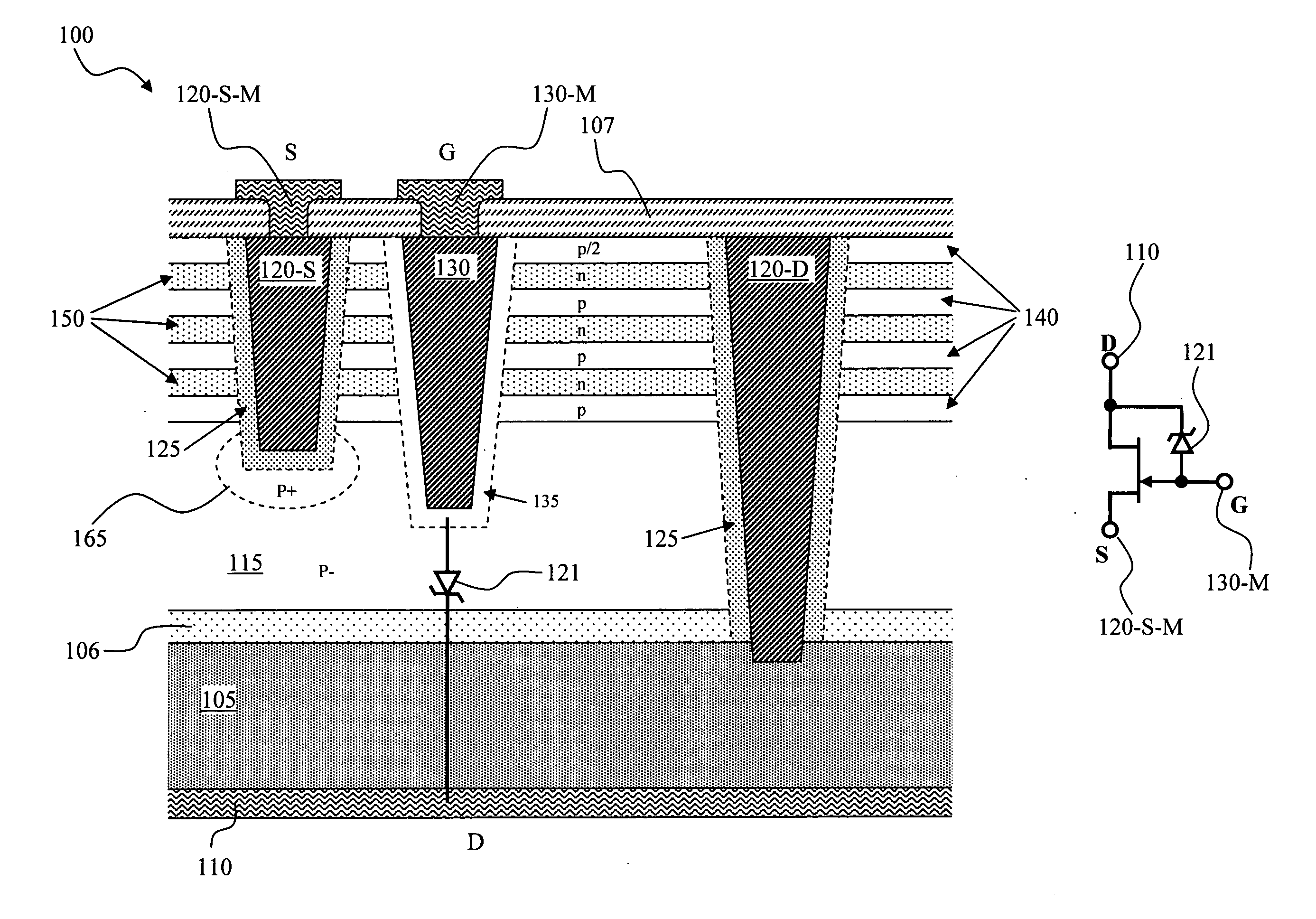
[0031]FIG. 2 is a cross sectional view of a lateral super junction high-voltage (HV) JFET device 100 having a bottom drain substrate of the present invention. The lateral JFET device 100 is supported on a P-Epitaxial layer 115 and an optional N buffer region 106 on an N+ substrate 105 functioning as a drain. The lateral JFET device 100 includes a drain metal electrode 110 disposed on the bottom of the substrate 105. The lateral power device 100 further includes an N source column 120-S and an N drain column 120-D formed respectively as first and second conductive columns disposed in a first trench and a second trench respectively on two opposite sides on the substrate. In this embodiment, each of these source and drain trenches may comprise a conductive material in the trench such as a metal fill or polysilicon surrounded by an N+ doped region 125. Of course, any other scheme may be utilized to form the N+ drain and source columns 120-D and 120-S. The N+ source column 120-S contacts...


PUM


Abstract

A lateral super junction JFET is formed from stacked alternating P type and N type semiconductor layers over a P-epi layer supported on an N+ substrate. An N+ drain column extends down through the super junction structure and the P-epi to connect to the N+ substrate to make the device a bottom drain device. N+ source column and P+ gate column extend through the super junction but stop at the P-epi layer. A gate-drain avalanche clamp diode is formed from the bottom the P+ gate column through the P-epi to the N+ drain substrate.

Description

[0001]This Patent Application is a Continuation in Part (CIP) Application of a co-pending Application with a Ser. No. 12 / 592,619 filed by a common Inventor of this Application on Nov. 30, 2009. The disclosure made in that Application is hereby incorporated by reference.BACKGROUND OF THE INVENTION[0002]1. Field of the Invention[0003]The invention relates generally to semiconductor power devices. More particularly, this invention relates to configurations and methods to manufacture lateral power device including a super-junction structure with an avalanche clamp diode formed between the drain substrate and the gate. The lateral super-junction structure reduces on-resistance, while the structural enhancements increase the breakdown voltage between substrate and drain and improve unclamped inductive switching (UIS) performance[0004]2. Description of the Prior Art[0005]Conventional semiconductor power device such as the MOSFET power devices implemented with a super-junction structure can...

Claims


Application Information

Patent Timeline
Patent Type & Authority Applications(United States)
IPC IPC(8): H01L27/06H01L21/8232
CPCH01L29/0626H01L29/808H01L29/0696H01L29/0843H01L29/0878H01L29/0882H01L29/1066H01L29/1095H01L29/4175H01L29/41766H01L29/4238H01L29/66696H01L29/66901H01L29/7817H01L29/7821H01L29/0634
Inventor BOBDE, MADHURGUAN, LINGPENGBHALLA, ANUPYILMAZ, HAMZA
Owner ALPHA & OMEGA SEMICON INC
Why Eureka
Try Eureka