Image-forming method
a technology of image and forming method, applied in the field of image forming method, can solve the problems of reduced image quality, large power as standby power, photosensitive member, etc., and achieve the effect of improving image quality and speed
- Summary
- Abstract
- Description
- Claims
- Application Information
AI Technical Summary
Benefits of technology
Problems solved by technology
Method used
Image
Examples
example 1
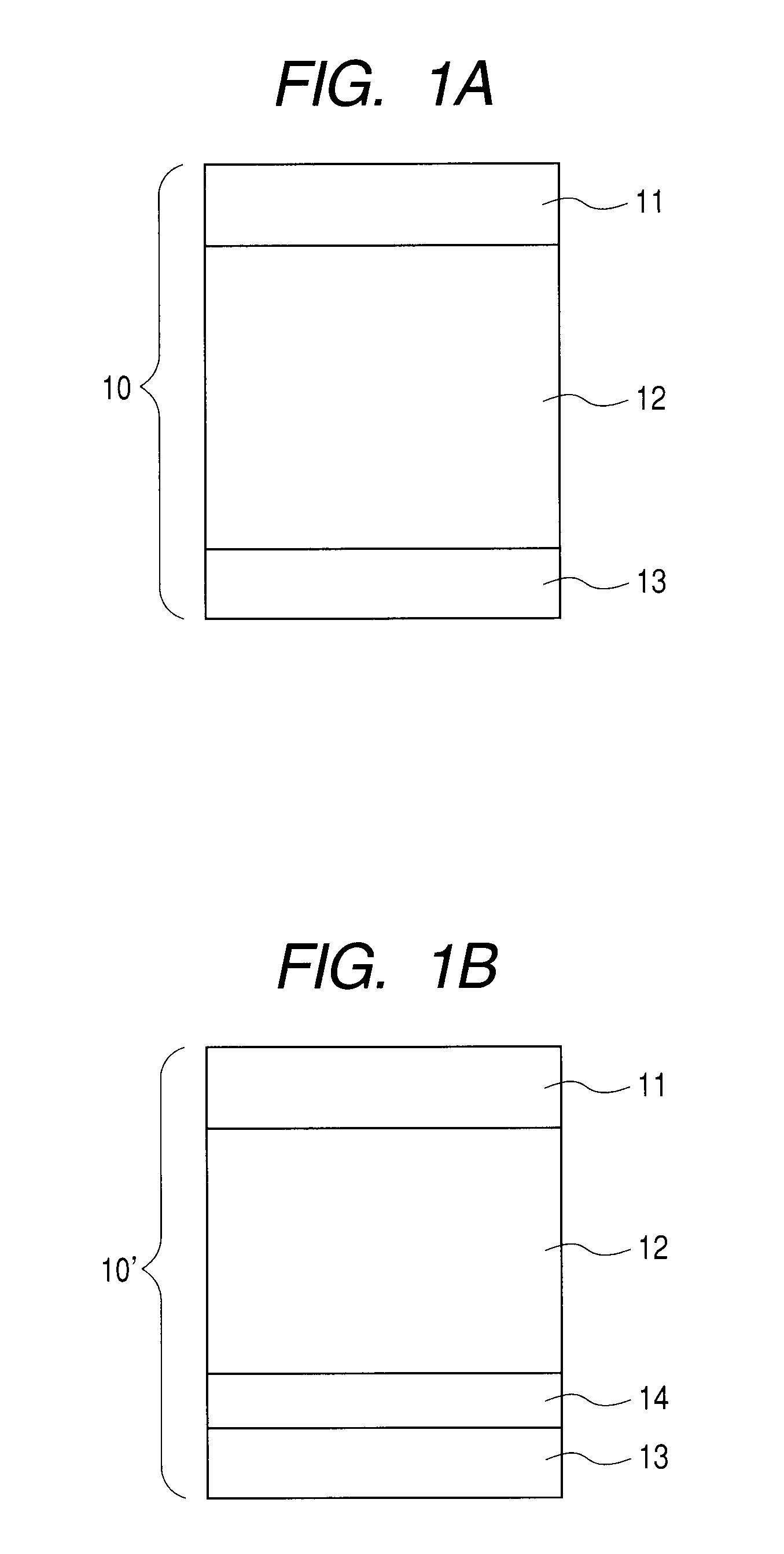
[0117]A photosensitive member of such a layer constitution (constitution illustrated in FIG. 1B) as to have a charge injection-blocking layer, a photoconductive layer, and a surface layer on a substrate was produced.
[0118]A cylinder obtained by subjecting the surface of an aluminum material having an outer diameter of 80 mm, a length of 358 mm, and a thickness of 3 mm to mirror finish was used as the substrate (conductive substrate), and the respective layers were formed under the conditions (film-forming conditions) shown in Table 1. In particular, with regard to the surface layer, layers having different densities were formed by changing the conditions (film-forming conditions) as shown in Table 2. It should be noted that thicknesses in Table 1 represents design values.
TABLE 1Chargeinjection-blockingPhotoconductiveSurfacelayerlayerlayerSpecies and flow rates of gasesSiH4 [mL / min (normal)]350450*H2 [mL / min (normal)]7502,200B2H6 [ppm] (with respect to1,5001SiH4)NO [mL / min (normal)]1...
example 2
[0190]A photosensitive member was produced in the same manner as in Example 1 except that the surface layer was formed while the gas species, the internal pressure, and the high-frequency power were changed to the conditions (film-forming conditions) shown in Table 6. The characteristics of the resultant photosensitive member were measured, and the photosensitive member was installed in an electrophotographic apparatus. Then, an image formed with the apparatus was evaluated. Table 8 shows the results.
TABLE 6Film-forming conditions No.7891011SiH4 [mL / min (normal)]3526262015CH4 [mL / min (normal)]190150190360400Internal pressure [Pa]7070707070High-frequency power [W]750800700900900
example 3
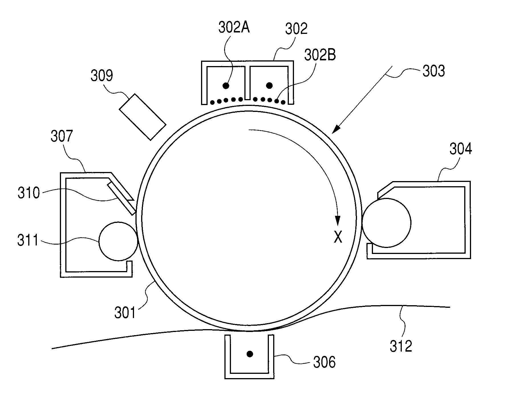
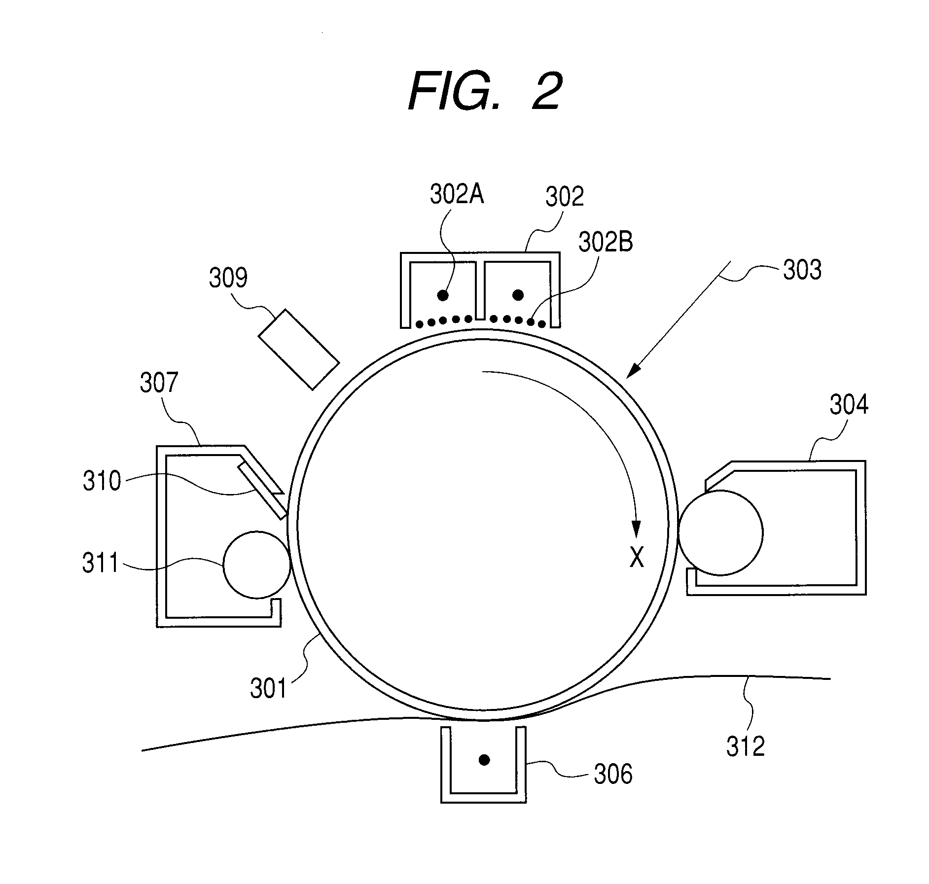
[0194]An image evaluation was performed in the same manner as in Example 1 except that photosensitive members in each of which the surface layer was formed under the film-forming conditions No. 2 in Example 1 with its thickness alone changed were used, and the laser device used for the image exposure in the modified machine B was replaced with a laser device having a peak wavelength shown in Table 9. Table 9 shows the results. It should be noted that the characteristics of the photosensitive members, which have been already shown in Table 5, are omitted.
TABLE 9Example 3Film-forming conditions No.2SurfaceThickness (nm)491495490499layerHigh humidity image deletion1.00resistanceAbrasion resistance1.01Image blurring0.98Peak wavelength of image635650658670exposure light (nm)Peak wavelength of pre-exposure630630630630light (nm)Wavelength difference (nm)5202840Charging performance0.991.011.020.98Photosensitivity1.091.051.040.98Ghost resistance1.091.030.981.00Oxidation resistance (reflectiv...
PUM
| Property | Measurement | Unit |
|---|---|---|
| peak wavelength | aaaaa | aaaaa |
| peak wavelength | aaaaa | aaaaa |
| peak wavelength | aaaaa | aaaaa |
Abstract
Description
Claims
Application Information


