Semiconductor device and switching regulator using the device

a switching regulator and semiconductor technology, applied in the direction of electric variable regulation, process and machine control, instruments, etc., can solve the problems of increasing the size and cost of the switching power supply icb>200/b>, reducing the size and cost of the switching regulator, and being more resistant to high voltage. , the effect of preventing the increase in size and cos

Active Publication Date: 2011-06-09
ROHM CO LTD
View PDF4 Cites 78 Cited by
  • Summary
  • Abstract
  • Description
  • Claims
  • Application Information

AI Technical Summary

Benefits of technology

[0013]With the semiconductor device thus configured, the entire device can be made more resistant to high voltage while being prevented from increasing in size and cost, making it possible to contribute to reducing the size and cost of a switching regulator obtained using this device.

Problems solved by technology

A problem is therefore encountered in that the switching power supply IC200 becomes larger and more expensive.

Method used


Image

  • Semiconductor device and switching regulator using the device
  • Semiconductor device and switching regulator using the device
  • Semiconductor device and switching regulator using the device

Examples


first embodiment

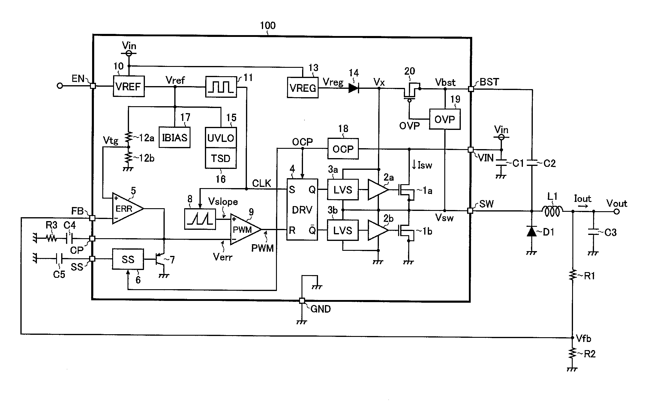
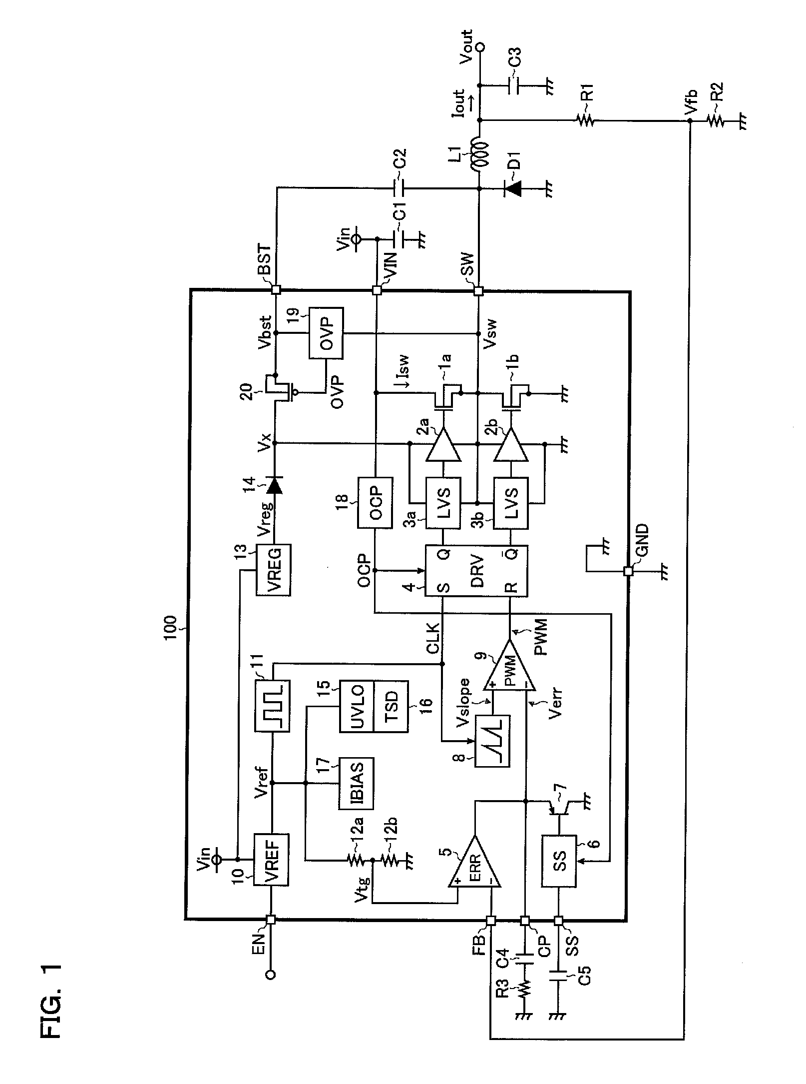
[0029]FIG. 1 is a circuit block diagram depicting a first embodiment of the switching regulator. As illustrated, the switching regulator of the first embodiment is a step-down switching regulator (chopper regulator) having a switching power supply IC 100, as well as an external inductor L1, a diode D1, resistors R1 to R3, and capacitors C1 to C5, and is adapted to generate a desired output voltage Vout from an input voltage Vin.

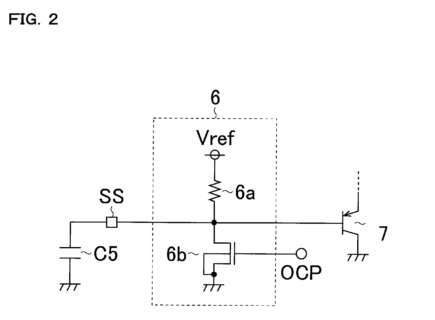
[0030]The switching power supply IC 100 has n-channel MOS field effect transistors 1a and 1b, drivers 2a and 2b, level shifters 3a and 3b, a drive control circuit 4, an error amplifier 5, a soft start control circuit 6, a pnp bipolar transistor 7, a slope voltage generation circuit 8, a PWM (Pulse Width Modulation) comparator 9, a reference voltage generation circuit 10, an oscillator 11, resistors 12a and 12b, a boosting constant voltage generation circuit 13, a diode 14, an undervoltage lockout circuit 15, a thermal shutdown circuit 16, an input bias curren...

second embodiment

[0071]A conventional switching regulator (a BUCK converter using a bootstrap system) depicted in FIG. 11 has a configuration wherein the transistor 201b connected between the switch terminal SW and the ground terminal GND undergoes switching control in complementary fashion to that of a transistor 201a.

[0072]With the conventional configuration shown above, in the event that the switching current Isw drops at times of low load or no load, resulting in a condition in which ringing noise arises in the switching voltage Vsw (so-called discontinuous current mode), the ringing noise may indeed escape to the ground terminal GND through the transistor 201b. Specifically, when the transistor 201a is OFF, the switching voltage Vsw is reduced to a low level (0 V) via the transistor 201b, and the capacitor C2 connected between the bootstrap terminal BST and the switch terminal SW can be adequately charges. Therefore, when the transistor 201a subsequently is switched ON, the boost voltage Vbst ...

third embodiment

[0084]In the conventional switching regulator depicted in FIG. 11, fluctuation in the output voltage Vout is initially detected by the error amplifier 205 when the load fluctuates, and the duty of the pulse width modulation signal PWM is expanded in association with the rise of the error voltage Verr so that the output voltage Vout is maintained at the target value.

[0085]With the above-described conventional configuration, fluctuations in the output voltage Vout can indeed be kept to a minimum when the load has relatively moderate fluctuations.

[0086]However, with the above-described conventional configuration, output feedback control by the PWM method is performed after fluctuation in the output voltage Vout is detected by the error amplifier 205. Therefore, the load response speed is low, and the problem of large fluctuations in the output voltage Vout during sudden changes in load sometimes occurs. Increasing the load response speed requires increasing the operating frequency of o...


PUM


Abstract

The semiconductor device according to the present invention has an n-channel output transistor wherein an input voltage is impressed on a drain, and a pulsed switching voltage that corresponds to a switching drive of the transistor is brought out from a source; a bootstrap circuit for generating a boost voltage enhanced by a predetermined electric potential above the switching voltage; an internal circuit for receiving a supply of the boost voltage to generate a switching drive signal, and supplying the signal to a gate of the output transistor; an overvoltage protection circuit for monitoring an electric potential difference between the switching voltage and the boost voltage, and generating an overvoltage detection signal; and a switching element for establishing/blocking electrical conduction between the internal circuit and the end impressed with the boost voltage, in accordance with the overvoltage detection signal.

Description

CROSS-REFERENCE TO RELATED APPLICATIONS[0001]This application is based on Japanese Patent Application No. 2009-279411 filed on Dec. 9, 2009, and Japanese Patent Application No. 2010-217437 filed on Sep. 28, 2010, the contents of which are hereby incorporated by reference.BACKGROUND OF THE INVENTION[0002]1. Field of the Invention[0003]The present invention relates to a semiconductor device for performing the switching drive control of an output transistor, and to a switching regulator using this device.[0004]2. Description of Related Art[0005]FIG. 11 is a circuit block diagram depicting a conventional switching regulator. As shown in FIG. 11, an n-channel MOS (metal oxide semiconductor) field effect transistor 201a is used as the output transistor in the conventional switching regulator, and a gate voltage greater than the input voltage Vin is needed in order to switch on the transistor 201a. In view of this, the conventional switching regulator is provided with a bootstrap circuit (...

Claims


Application Information

Patent Timeline
Patent Type & Authority Applications(United States)
IPC IPC(8): G05F1/00
CPCH03K17/0822H02M3/156H02M1/32H02M1/08
Inventor MURAKAMI, KAZUHIRODOI, MIKIYAFUKUMOTO, YOSUKE
Owner ROHM CO LTD
Why Eureka
Try Eureka