Analog-to-digital converter

a converter and analog-to-digital technology, applied in analogue/digital conversion, transmission systems, instruments, etc., can solve the problems of mismatch of input-convertible offset between two comparators, deterioration of precision, and increase in circuit size accordingly, so as to increase the allowable range of offset mismatch, the number of comparison processing steps, and the number of reference capacitors.

Inactive Publication Date: 2011-06-09
SEMICON TECH ACADEMIC RES CENT
View PDF5 Cites 25 Cited by
  • Summary
  • Abstract
  • Description
  • Claims
  • Application Information

AI Technical Summary

Benefits of technology

[0041]An object of the present invention is to realize an SAR ADC that has a simple configuration and meets the demands of high speed, high precision, and low power consumption.
[0048]According to the present invention, the redundant non-binary algorithm is applied, and therefore, the number of times of comparison processing (steps) and the number of the reference capacitors increase somewhat; however, it is possible to increase the allowable range of the offset mismatch of the two comparators.
[0049]According to the present invention, it is possible to improve precision of the SAR ADC capable of high-speed operations and having a low power consumption.

Problems solved by technology

However, the method proposed in V. Giannini, P. Nuzzo, V. Chironi, A. Baschirotto, G. V. Plas, J. Craninckx “An 820 μW 9b 40MS / s Noise-Tolerant Dynamic-SAR ADC in 90 nm Digital CMOS” ISSCC (February 2008) has such a problem that precision is deteriorated by a mismatch of an input-converted offset between two comparators.
However, when the variable capacitors VRp and VRn are provided, the size of the circuit is increased accordingly and such a problem arises that it is necessary to provide an offset adjusting process in the manufacturing process and the cost is increased accordingly.

Method used


Image

  • Analog-to-digital converter
  • Analog-to-digital converter
  • Analog-to-digital converter

Examples


first embodiment

[0071]FIG. 10A to FIG. 10C are diagrams explaining an operation example when the SAR ADC in the first embodiment is assumed to be a 5-bit DAC. Because of five bits, the AD converted values have 32 levels from 0 to 31.

[0072]When the shift weight is binary, five steps of comparison operation are performed in the 5-bit DAC; however, in the SAR ADC in the first embodiment, as shown in FIG. 10A, six steps of comparison operation are performed. Then, in first to third steps, the first comparator 21 with low power consumption but high noise is used and in fourth to sixth steps, the second comparator 22 with high power consumption but low noise is used. In FIG. 8, in the first to third steps, the operating state selection circuit 24 supplies the signal Comp to the first comparator 21 and the selector 25 selects the output of the first comparator 21. In the first to third steps, the second comparator 22 is in the non-operating state. In the fourth to sixth steps, the operating state selectio...

second embodiment

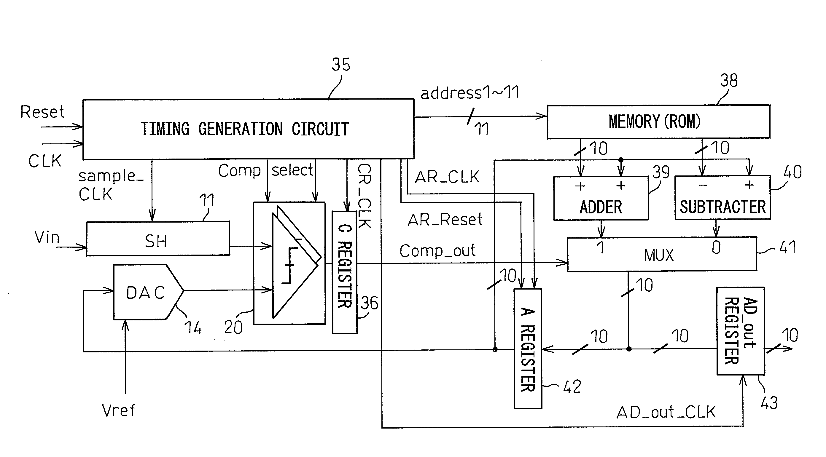
[0078]FIG. 11 is a diagram showing a configuration of a 10-bit SAR ADC in the present invention.

[0079]The 10-bit charge-sharing SAR ADC in the second embodiment comprises the DAC 14, the comparator unit 20, a timing generation circuit 35, a C register 36, a memory 38, an adder 39, a subtracter 40, a multiplexer 41, an A register 42, and an AD_out register 43. The sample-holding circuit (SH) 11, the DAC 14, and the comparator unit 20 are the same as those in the first embodiment and the comparator unit 20 has the first comparator 21 and the second comparator 22. The timing generation circuit 35, the C register 36, the memory 38, the adder 39, the subtracter 40, the multiplexer 41, the A register 42, and the AD_out register 43 form the part corresponding to the control circuit 23 in the first embodiment.

[0080]The timing generation circuit 35 receives a reset signal Reset and a clock CLK and generates and outputs a timing signal sample_CLK, the timing signals Comp, select, and timing s...

third embodiment

[0104]As shown in FIG. 13, the charge-sharing SAR ADC in the third embodiment comprises a comparison processing part 51 having a C_array 52 and the comparator unit 20, a timing generation circuit 55, a C register 56, a shift register 57, a memory 58, an adder 59, a subtracter 60, the multiplexer 61, an A register 62, and an AD_out register 63. The parts except for the comparison processing part 51 form the part corresponding to the control circuit 17 in FIG. 3.

[0105]As shown in FIG. 14, the C_array 52 comprises the switch SW1, the input signal capacitor Cs, and 10 reference capacitor circuits 53-1, . . . , 53-10. As shown in FIG. 14, the configuration of each reference capacitor circuit has the same configuration as that of the conventional charge-sharing SAR ADC shown in FIG. 3. However, the conventional n-bit charge-sharing SAR ADC comprises n−1, i.e., nine reference capacitor circuits in the case of 10 bits; however, the 10-bit charge-sharing SAR ADC in the present embodiment dif...


PUM


Abstract

An SAR ADC includes a digital-to-analog converter, a first comparator that compares an input analog signal with a reference analog signal, a second comparator that compares an input analog signal with a reference analog signal, a selection circuit that selects one of comparison results of the first comparator and the second comparator, and a control circuit that changes the multibit digital signal sequentially based on the selected comparison result in a plurality of steps so that the reference analog signal becomes closer to the input analog signal, and the control circuit controls the selection circuit to select the comparison result of the first comparator up to an intermediate step on the way of the plurality of steps and to select the comparison result of the second comparator after the intermediate step, and changes the bit value of the multibit digital signal according to the non-binary algorithm.

Description

CROSS-REFERENCE TO RELATED APPLICATIONS[0001]This application is based upon and claims the benefit of priority of the prior Japanese Patent Application No. 2009-275716, filed on Dec. 3, 2009, the entire contents of which are incorporated herein by reference.BACKGROUND OF THE INVENTION[0002]1. Technical Field of the Invention[0003]The present invention relates to a sequential comparison-type analog-to-digital converter (SAR ADC: Successive Approximation Register Analog-to-Digital Converter).[0004]2. Related Art[0005]A sequential comparison-type analog-to-digital converter (ADC) mounted on a microcomputer or system LSI, is used from the viewpoint of downsizing and maintaining high precision.[0006]FIG. 1 is a block diagram showing a configuration example of a conventional SAR ADC. FIG. 2 is a diagram for explaining a conversion operation in the SAR ADC.[0007]As shown in FIG. 1, the conventional SAR ADC comprises a comparator 12, a control circuit 13, and a DA converter (digital-to-anal...

Claims


Application Information

Patent Timeline
Patent Type & Authority Applications(United States)
IPC IPC(8): H03M1/12
CPCH03M1/0678H03M1/468H03M1/462H03M1/069
Inventor OGAWA, TOMOHIKOKOBAYASHI, HARUO
Owner SEMICON TECH ACADEMIC RES CENT
Why Eureka
Try Eureka