Semiconductor device and manufacturing method thereof

a technology of a semiconductor and a manufacturing method, applied in the field of semiconductor devices, can solve the problems of easy variation, increase of leak current under reverse biased state, and recombination degree of electrons and holes, and achieve the effect of lowering the reverse recovery charge (qrr) and softening the recovery curren

Inactive Publication Date: 2011-06-16
TOYOTA JIDOSHA KK
View PDF3 Cites 21 Cited by
  • Summary
  • Abstract
  • Description
  • Claims
  • Application Information

AI Technical Summary

Benefits of technology

[0006]In general, an energy level of the crystal defects is a recombination center for electrons and holes, and also a generation center for electrons and holes when a high electrical field is applied (a reverse biased state). Therefore, if many crystal defects are formed within the semiconductor substrate, an increase of leak current may occur under the reverse biased state. It is known that crystal defects formed by using the diffusion of the heavy metal have a low generation degree of electrons and holes (the generation degree of electrons and holes hereinafter referred to as “a generation probability”). Therefore, the leak current is repressed in the case where the type of crystal defects formed within the semiconductor substrate is originated from the diffusion of the heavy metal. However,...

Problems solved by technology

Therefore, if many crystal defects are formed within the semiconductor substrate, an increase of leak current may occur under the reverse biased state.
However, the crystal defects formed by using the diffusion of the heavy metal has a problem that a recombination degree of electrons and holes (hereinafter referred to as “a recombination probability”) easily varies based on a temperature.
In the above mentioned prior art, both types of crystal defects formed by using the diffusion of the heavy metal and irradiation of the charged particl...

Method used


Image

  • Semiconductor device and manufacturing method thereof
  • Semiconductor device and manufacturing method thereof
  • Semiconductor device and manufacturing method thereof

Examples


Embodiment Construction

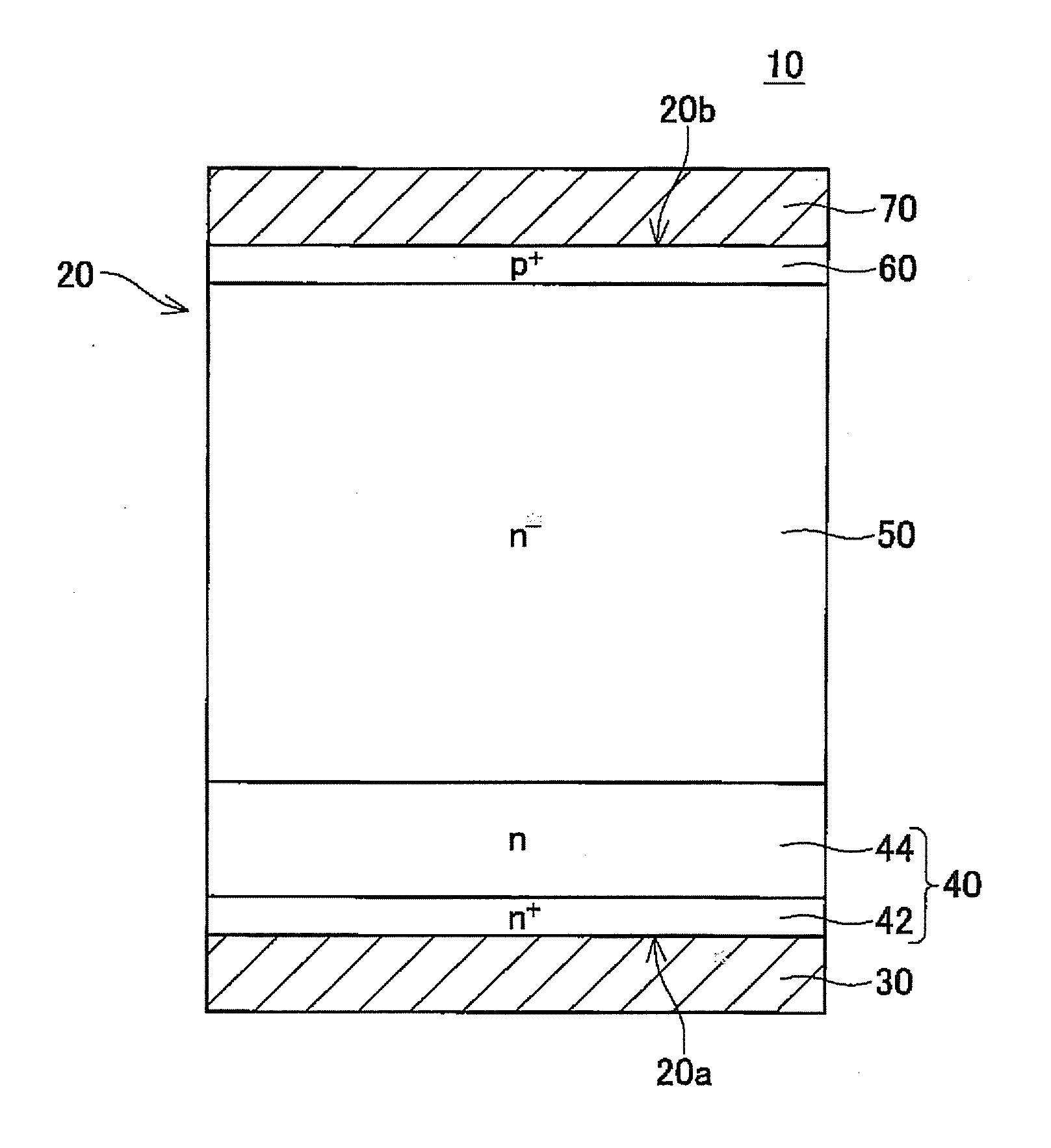
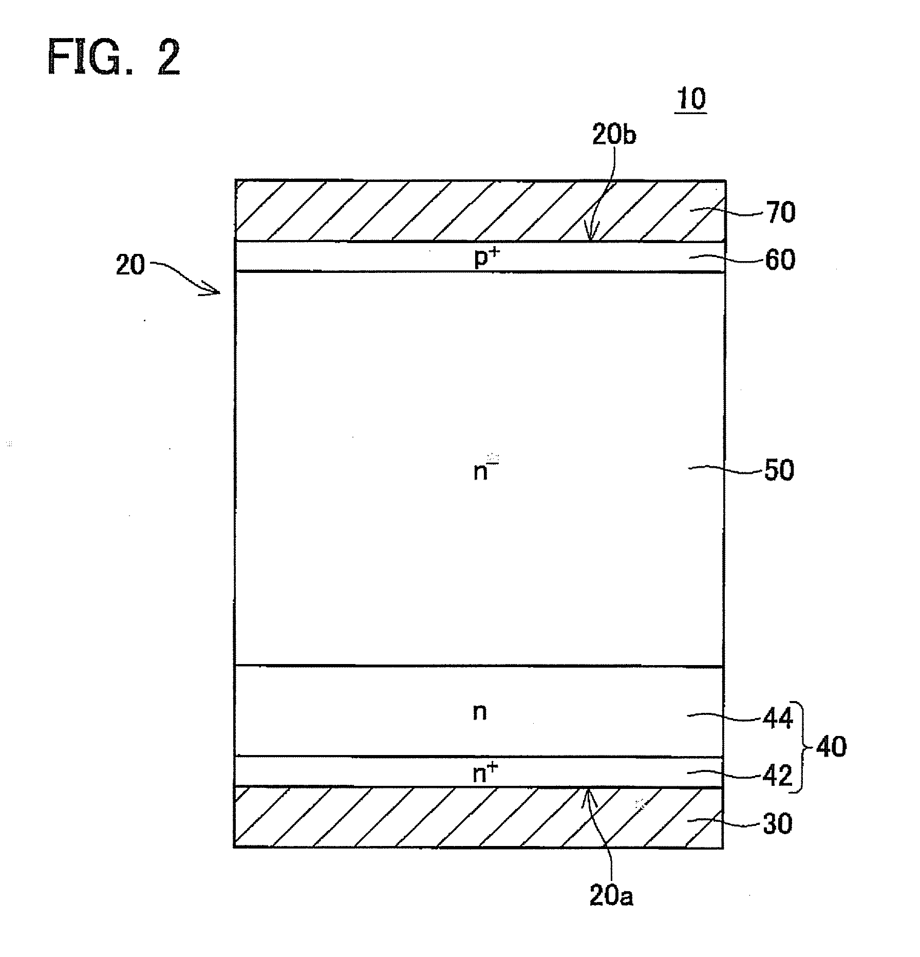
[0027]FIG. 2 shows a schematic cross sectional view of a diode 10. Note that FIG. 2 only depicts an element region and does not depict a terminal region disposed around the element region. The diode 10 comprises a semiconductor substrate 20 of monocrystal silicon, a cathode electrode 30 formed on a first main surface 20a of the semiconductor substrate 20 and an anode electrode 70 formed on a second main surface 20b of the semiconductor substrate 20. The diode 10 belongs to a so-called vertical type PIN diode.

[0028]As shown in FIG. 2, the semiconductor substrate 20 comprises a cathode region 42, an electrical field inhibition region 44 formed on the cathode region 42, a voltage maintaining region 50 formed on the electrical field inhibition region 44 and an anode region 60 formed on the voltage maintaining region 50. The cathode region 42 and the electrical field inhibition region 44 include a higher density of n-type impurities than the voltage maintaining region 50. The cathode reg...


PUM


Abstract

A semiconductor device comprises a semiconductor substrate, a first electrode formed on a first main surface of the semiconductor substrate, and a second electrode formed on a second main surface of the semiconductor substrate. The semiconductor substrate includes a first region in which a density of oxygen-vacancy defects is greater than a density of vacancy cluster defects, and a second region in which the density of vacancy cluster defects is greater than the density of oxygen-vacancy defects.

Description

CROSS-REFERENCE TO RELATED APPLICATIONS[0001]This application claims priority to Japanese Patent Application No. 2009-285078 filed on Dec. 16, 2009 and Japanese Patent Application No. 2010-169360 filed on Jul. 28, 2010, the contents of which are hereby incorporated by reference into the present application.TECHNICAL FIELD[0002]The present invention relates to a semiconductor device. The present invention, in particular, relates to a free wheel diode which is connected to a power semiconductor device in an inverse-parallel connection.DESCRIPTION OF RELATED ART[0003]A diode is used in many types of electrical circuits, and its function covers widespread fields. For example, the diode is used in an inverter circuit which controls a supply of an electrical power to a load. The inverter circuit comprises a plurality of power semiconductor devices being in bride connection, and diodes are connected to these power semiconductor devices in an inverse-parallel connection respectively. This t...

Claims


Application Information

Patent Timeline
IPC IPC(8): H01L29/30H01L21/322
CPCH01L21/263H01L21/26506H01L29/32Y10S438/92H01L29/861H01L29/868H01L21/02238H01L29/6609
Inventor MISUMI, TADASHIIWASAKI, SHINYASUGIYAMA, TAKAHIDE
Owner TOYOTA JIDOSHA KK
Why Eureka
Try Eureka