Flash Memory Device and Method for Manufacturing Flash Memory Device

a flash memory and flash memory technology, applied in the direction of digital storage, semiconductor devices, instruments, etc., can solve the problems of increasing the voltage needed for the erasing process, the erasing process efficiency of the sonos memory device, and the erasing time, so as to minimize the influence of stress and disturbance, and achieve the effect of effective realizing the operating voltage application

Inactive Publication Date: 2011-06-16
COLUMBA TECH INC
View PDF1 Cites 12 Cited by
  • Summary
  • Abstract
  • Description
  • Claims
  • Application Information

AI Technical Summary

Benefits of technology

[0012]Embodiments provide a flash memory device that can be composed of a variety of cell arrays without an odd-even characteristic, effectively realize operating voltage application, and minimize influence of stress and disturbance that occur during a cell arraying operation.

Problems solved by technology

Accordingly, the SONOS memory device has lower erasing process efficiency.
However, when a thickness of the tunnel oxide increases, an erasing time increases or a voltage necessary to perform the erasing process increases, and a back-tunneling phenomenon where the electrons are introduced from a gate to the insulation layer (tunnel oxide) occurs.
Meanwhile, since the charges are distributed within 100 nm of the ion injection area, the insulation area outside of the charge distribution area is unnecessary.
That is, the insulation area outside of the charge distribution area causes the increase of erasing voltage and the decrease of cell current.
However, the former case has a limitation in that, since it is difficult to define a critical dimension and removal area in a photolithography process, chips have different properties.
The latter case has a limitation in that the process is complicated and the cell property may be deteriorated.
Thus, an endurance property is deteriorated.

Method used


Image

  • Flash Memory Device and Method for Manufacturing Flash Memory Device
  • Flash Memory Device and Method for Manufacturing Flash Memory Device
  • Flash Memory Device and Method for Manufacturing Flash Memory Device

Examples


Embodiment Construction

[0034]Reference will now be made in detail to certain embodiments of the present disclosure, examples of which are illustrated in the accompanying drawings.

[0035]In the description of embodiments, it will be understood that when a layer (or film) is referred to as being ‘on’ another layer or substrate, it can be directly on another layer or substrate, or intervening layers may also be present. Further, it will be understood that when a layer is referred to as being ‘under’ another layer, it can be directly under another layer, or one or more intervening layers may also be present. In addition, it will also be understood that when a layer is referred to as being ‘between’ two layers, it can be the only layer between the two layers, or one or more intervening layers may also be present.

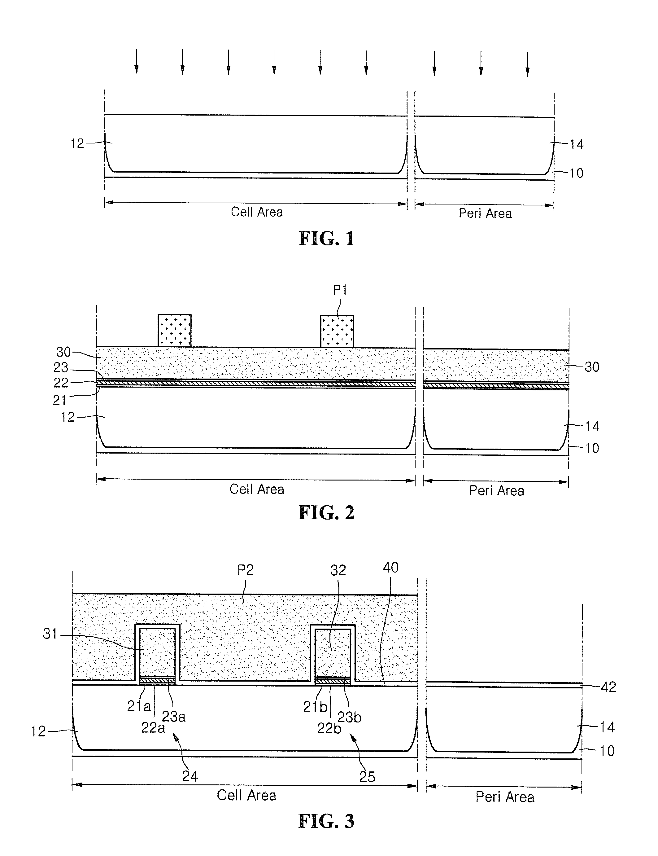
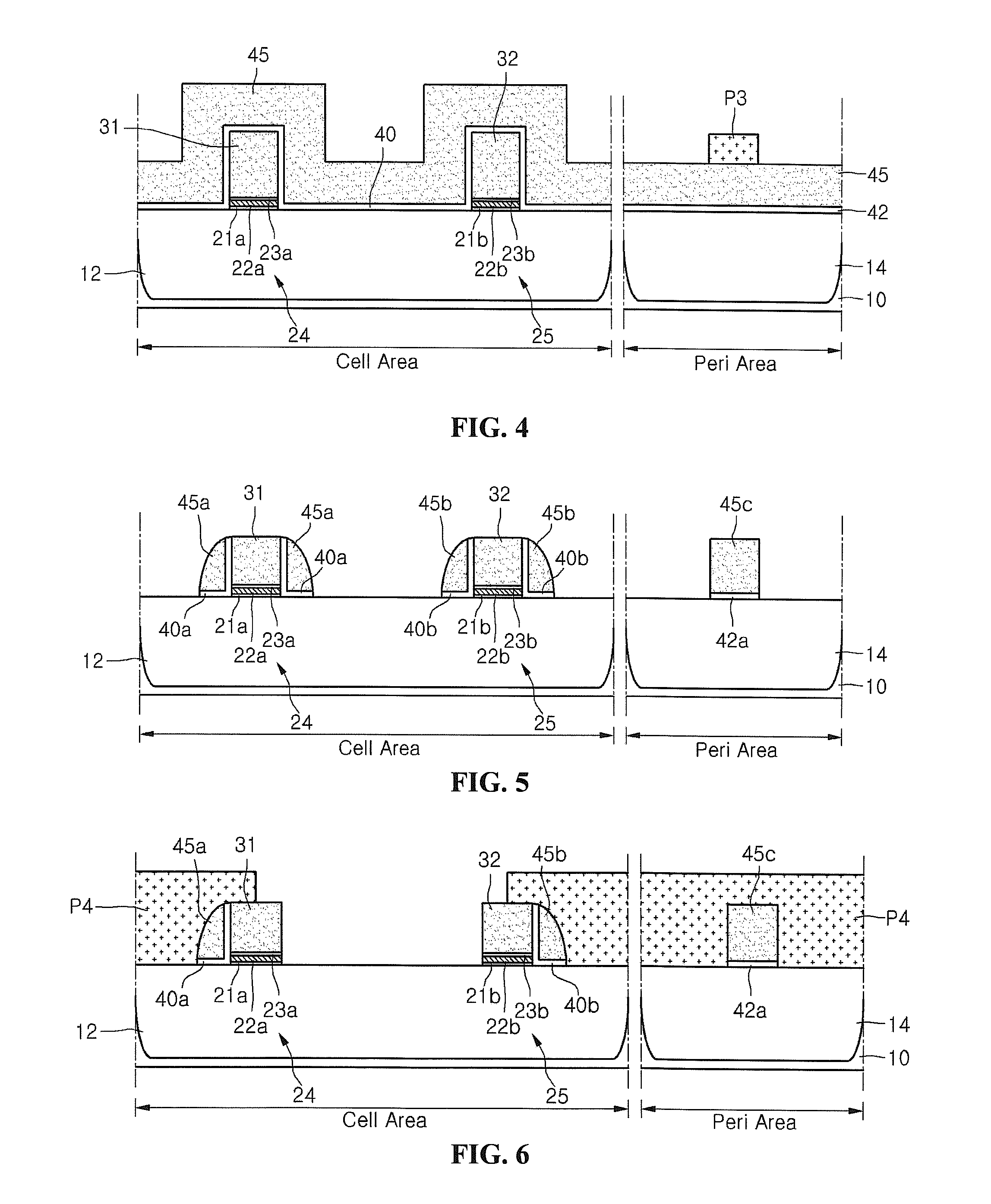
[0036]FIGS. 1-11 illustrate a method for manufacturing a flash memory device according to an embodiment.

[0037]As shown in FIG. 1, a semiconductor substrate 10 includes a cell area and a peripheral area....


PUM


Abstract

A method of manufacturing a flash memory device is provided. First and second gates are formed on first and second dielectrics and spaced apart from each other on a cell area of a substrate. A third gate is formed on a third dielectric that is formed on first opposing sidewalls of the first gate and extending on a portion of the substrate from the first opposing sidewalls. A fourth gate is formed on a fourth dielectric that is formed on second opposing sidewalls of the second gate and extending on a portion of the substrate from the second opposing sidewalls. The third gate and third dielectric on one of the first opposing sidewalls facing the second gate and the fourth gate and fourth dielectric on one of the second opposing sidewalls facing the first gate are removed. Drain areas are formed at outer sides of the third and fourth gates, and a common source area is formed between the first and second gates.

Description

CROSS-REFERENCE TO RELATED APPLICATIONS[0001]This application claims the benefit under 35 U.S.C. §119 of Korean Patent Application Nos. 10-2009-0125747, filed on Dec. 16, 2009, and 10-2010-0033237, filed on Apr. 12, 2010, which are hereby incorporated by reference in their entirety.BACKGROUND[0002]The present disclosure relates to a flash memory device and a method of manufacturing the flash memory device.[0003]A flash memory device is a non-volatile storage medium and thus no power is needed to maintain data stored therein. In addition, the flash memory device has an advantage of offering relatively fast process speeds such as fast programming speed, fast read access speed, and fast erasing speed.[0004]For the flash memory device, a semiconductor device using a silicon-oxide-nitride-oxide-silicon (SONOS) structure is often used. Many masks for forming patterns are used to manufacture the SONOS memory device.[0005]Charges injected into a dielectric (e.g., a nitride layer) of the SON...

Claims


Application Information

Patent Timeline
Patent Type & Authority Applications(United States)
IPC IPC(8): G11C16/06H01L21/336H01L29/78
CPCH01L27/11573G11C16/0441H10B43/40
Inventor KIM, DAE IL
Owner COLUMBA TECH INC
Why Eureka
Try Eureka