
Plasma processing apparatus

Active Publication Date: 2011-06-30
TOKYO ELECTRON LTD
View PDF43 Cites 168 Cited by
  • Summary
  • Abstract
  • Description
  • Claims
  • Application Information

AI Technical Summary

Benefits of technology

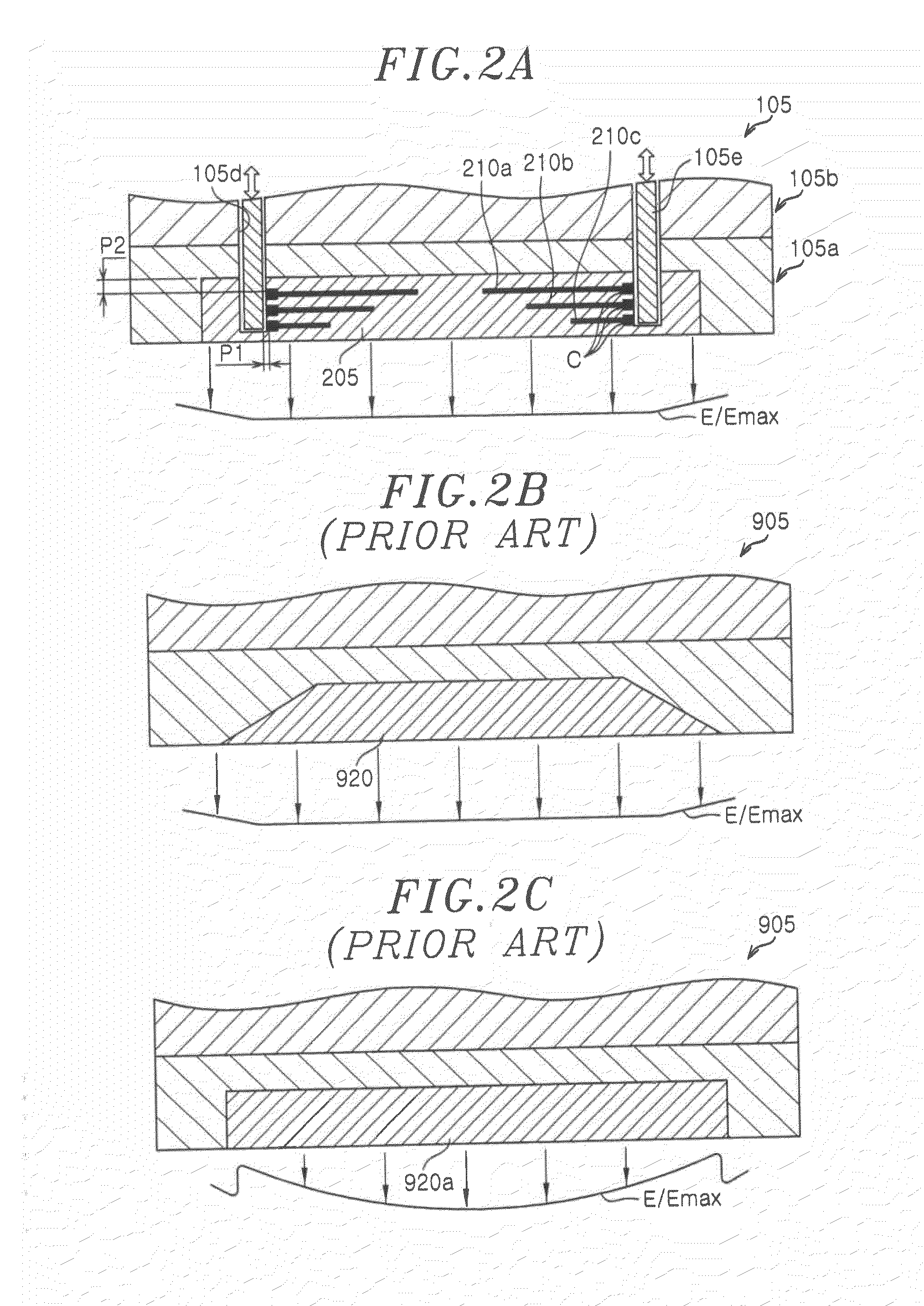
[0012]With the plasma processing apparatus, it is considered that the amount of currents flowing through the metal surfaces of the metal plate electrodes is approximately identical to that of a current flowing through the metal surface of the base. As a result, from the plasma side, the base and the respective plate electrodes are seen as if they are provided as a single unit. Accordingly, portions of the dielectric body located on the sides of the respective plate electrodes opposite to the plasma side are seen as if they were not provided. In other words, from the plasma side, it is seen that portions of the dielectric body on the rear sides of the plate electrodes are respectively interrupted by the plate electrodes. Accordingly, when all potentials of the plate electrodes are adjusted to the ground level, the capacitance component becomes larger at the end portion of the dielectric body than that at the central portion thereof. As a result, it is possible to obtain the uniform electric field intensity distribution at the end portions of the plate electrodes without significantly lowering the electric field intensity distribution E / Emax. In this way, it is possible to obtain the similar effect to the case of providing the taper-shaped dielectric body shown in FIG. 2B.

Problems solved by technology

However, in the case of the dielectric body 920 of the taper shape, the dimensional precision at the tapered portion may be deteriorated due to the machining work and, resultantly, the stress concentration occurs due to such thermal expansion difference.
Such stress concentration causes the adhesive on the adhesive interface to be peeled off and the peeled-off adhesive comes out of the gap, thereby polluting the inside of the chamber.

Method used


Image

  • Plasma processing apparatus
  • Plasma processing apparatus
  • Plasma processing apparatus

Examples


Embodiment Construction

[0024]An embodiment of the present invention will now be described in detail with reference to the accompanying drawings which form a part hereof. Further, in the following description and drawings, components having substantially the same configuration and function are denoted by like reference characters, and thus redundant description thereof will be omitted herein.

[0025](Configuration of Plasma Processing Apparatus)

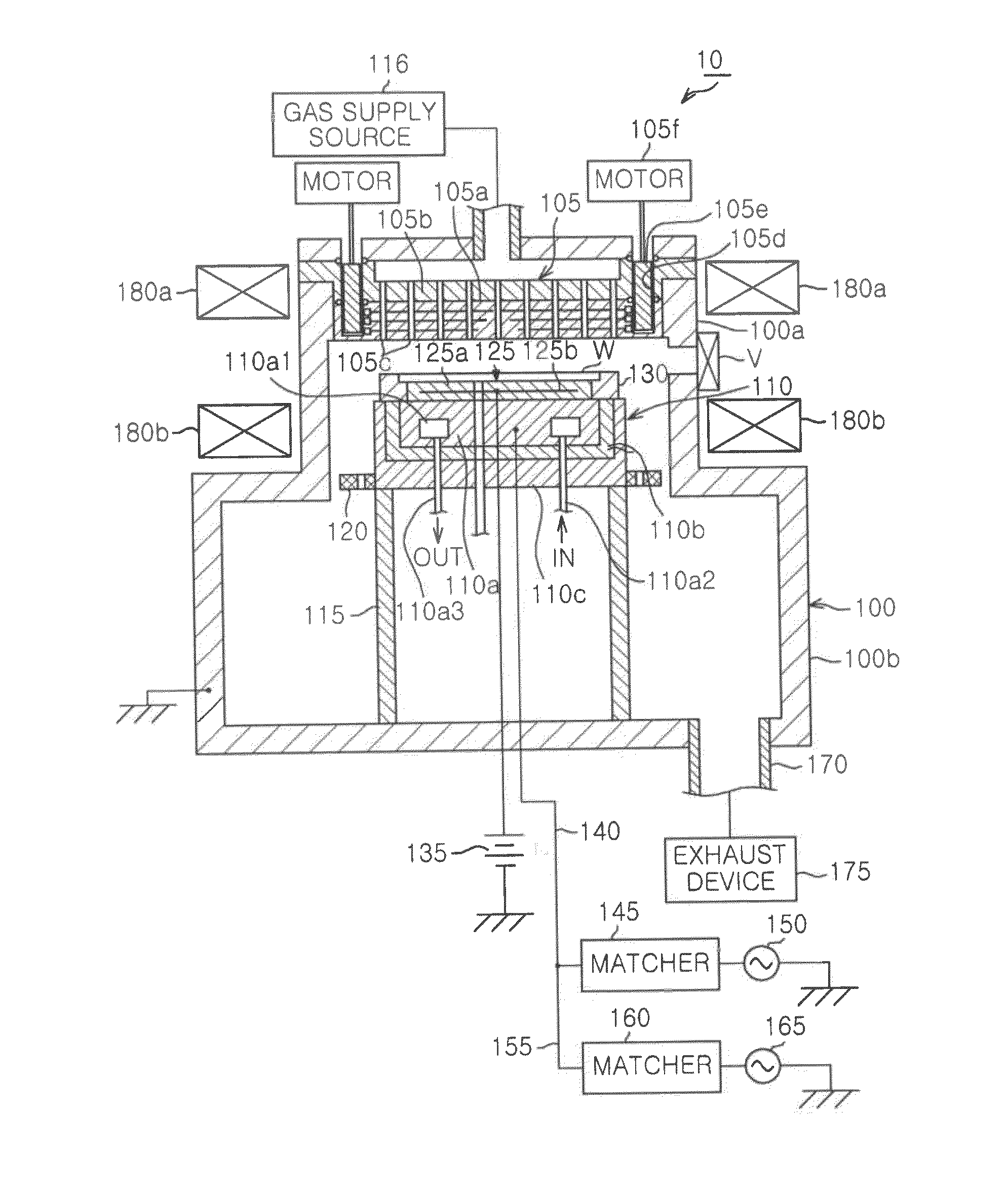
[0026]First, the configuration of a plasma processing apparatus in accordance with an embodiment of the present invention will be described with reference to FIG. 1. FIG. 1 is a longitudinal cross sectional view showing an RIE plasma etching apparatus (parallel plate plasma processing apparatus) 10 in accordance with the embodiment of the present invention. The RIE plasma etching apparatus 10 is taken as an example of a plasma processing apparatus for performing a desired plasma process on a target substrate to be processed.

[0027]The RIE plasma etching apparatus 10 in...


PUM

PropertyMeasurementUnit
Electrical resistanceaaaaaaaaaa
Electrical resistivityaaaaaaaaaa

Abstract

A plasma processing apparatus includes a processing chamber in which a target substrate is processed; an application electrode and a facing electrode provided to face each other in the processing chamber, a plasma generation space being formed between the application electrode and the facing electrode; and an RF power supply connected to the application electrode, an RF power being supplied from the RF power supply to the application electrode. At least one of the application electrode and the facing electrode includes a base formed of a metal, and a dielectric body inserted into the base, one or more metal plate electrodes being buried in the dielectric body.

Description

CROSS-REFERENCE TO RELATED APPLICATIONS[0001]This application claims priority to Japanese Patent Application No. 2009-297687 filed on Dec. 28, 2009 and U.S. Provisional Application No. 61 / 307,629 filed on Feb. 24, 2010, the entire contents of which are incorporated herein by reference.FIELD OF THE INVENTION[0002]The present invention relates to a plasma processing apparatus in which a predetermined plasma process is performed through the action of a plasma; and, more particularly, to a plasma processing apparatus including an electrode structure for controlling the intensity distribution of an electric field caused by an RF power consumed to generate a plasma.BACKGROUND OF THE INVENTION[0003]A capacitive coupled (parallel plate) plasma processing apparatus, an inductively coupled plasma processing apparatus, a microwave plasma processing apparatus or the like has been put to practical use in an apparatus for performing a micro process such as an etching process or a film forming pro...

Claims


Application Information

Patent Timeline
IPC IPC(8): C23F1/08
CPCH01J37/32091H01L21/67069H01J37/3255H01J37/32541H01J37/32577H01J37/32605
Inventor HIMORI, SHINJIHAYASHI, DAISUKESHIMIZU, AKITAKA
Owner TOKYO ELECTRON LTD
Learn More