Bulk silicon wafer product useful in the manufacture of three dimensional multigate mosfets

a technology of three-dimensional transistors and bulk wafers, which is applied in the direction of semiconductor/solid-state device testing/measurement, semiconductor devices, semiconductor/solid-state device details, etc., can solve the problems of bulk wafers presenting a transistor processing challenge, soi wafers not contributing to the improvement of the device performance of three-dimensional transistors, and so on. avoiding the potentially damaging effects of ion implantation methods

Active Publication Date: 2011-07-07
GLOBALWAFERS CO LTD
View PDF13 Cites 10 Cited by
  • Summary
  • Abstract
  • Description
  • Claims
  • Application Information

AI Technical Summary

Benefits of technology

[0008]Among the aspects of the present invention may be noted the provision of a method for preparing a silicon wafer suitable for use in the manufacture of three dimensional transistors. The silicon wafer comprises an endpoint detection region that is formed by epitaxial deposition, thereby avoiding the potentially damaging effects of ion implantation methods to form the endpoint detection layer.

Problems solved by technology

The SOI wafer, however, does not contribute to improved device performance of the three dimensional transistor.
Moreover, the use of SOI wafer is disadvantageous from a cost perspective compared to fabricating a three-dimensional transistor on a non-SOI bulk wafer.
Bulk wafers present a transistor processing challenge since they lack the built-in oxide etch stop available on the SOT wafer.
A negative effect occurs, however, when the implant species travels through the device region and disorders the silicon lattice.
Another potential disadvantage of ion implantation is the broad depth distribution of the ion implanted species, which may affect the ability of the subsequent etching process to define fins of precise heights.

Method used


Image

  • Bulk silicon wafer product useful in the manufacture of three dimensional multigate mosfets
  • Bulk silicon wafer product useful in the manufacture of three dimensional multigate mosfets
  • Bulk silicon wafer product useful in the manufacture of three dimensional multigate mosfets

Examples


Embodiment Construction

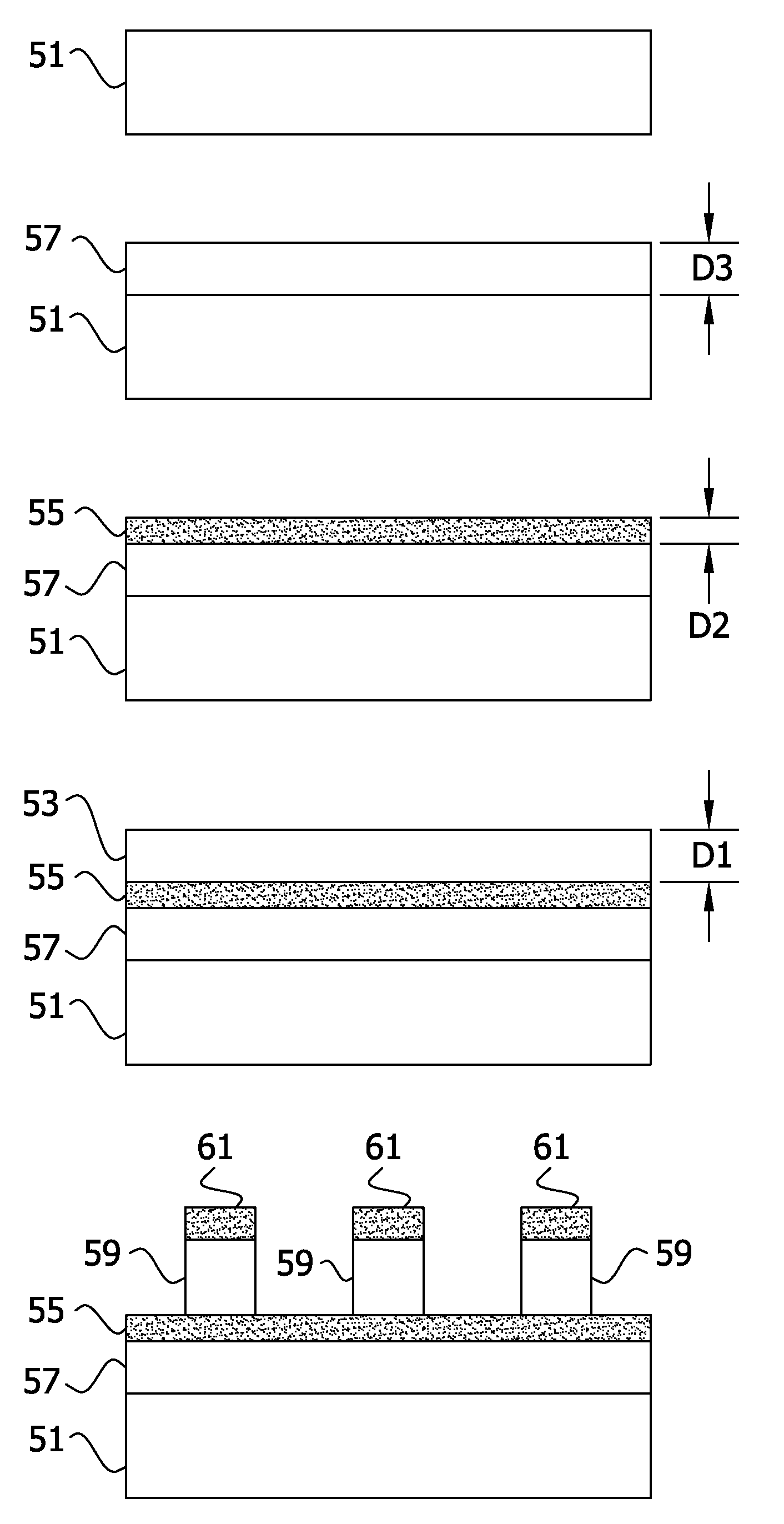
[0018]The present invention is directed to a method for preparing a semiconductor structure for the manufacture of three dimensional transistors. The semiconductor structure comprises a silicon wafer substrate and an epitaxial layer, the epitaxial layer comprising an endpoint detection region compatible with three dimensional transistor fabrication. Since the endpoint detection region is formed by epitaxial deposition, the fin height may be more precisely controlled. The semiconductor structure may be manufactured at a lower cost compared to the preparation of SOI wafers for use in manufacture of three dimensional transistors. Moreover, the semiconductor structure is not prepared by ion implantation methods that may potentially damage the silicon lattice structure. This further avoids the need for annealing the semiconductor structure post-implantation to repair the damage to the lattice structure and activate the implanted dopant atom.

[0019]In general, the semiconductor structure o...


PUM

PropertyMeasurementUnit
heightaaaaaaaaaa
average transverse distanceaaaaaaaaaa

Abstract

A method for preparing a semiconductor structure for use in the manufacture of three dimensional transistors, the structure comprising a silicon substrate and an epitaxial layer, the epitaxial layer comprising an endpoint detection epitaxial region comprising an endpoint detection impurity selected from the group consisting of carbon, germanium, or a combination.

Description

FIELD OF THE INVENTION[0001]The present invention relates to a method for producing a silicon wafer useful in the manufacture of three dimensional transistors.BACKGROUND OF THE INVENTION[0002]Three dimensional metal-oxide-semiconductor field-effect transistors (“MOSFETs”), often referred to as MultiGate FET (“MUGFETs”), “finFETs,” or “TriGate FETs,” are expected to be adopted in complementary metal-oxide-semiconductor (“CMOS”) device fabrication at the 32 nm technology node in order to alleviate issues with short channel effects. Manufacture of a three dimensional MOSFET requires masked etching of silicon to create a raised cuboid of silicon referred to in the art as a “fin” that serves as the body of the transistor. In the manufacture of the three dimensional transistor, control of the fin length, depth, and height are key process control factors. The typical height of the fin is between about 50 nm and about 100 nm. The means of controlling fin height depends upon the silicon wafe...

Claims


Application Information

Patent Timeline
Patent Type & Authority Applications(United States)
IPC IPC(8): H01L29/06H01L21/306
CPCH01L21/02573H01L21/3065H01L22/26H01L21/0262H01L21/02532H01L29/66795H01L29/06
Inventor SEACRIST, MICHAEL R.
Owner GLOBALWAFERS CO LTD
Why Eureka
Try Eureka