Integrated circuit micro-module

Active Publication Date: 2011-07-07
NAT SEMICON CORP
View PDF24 Cites 72 Cited by
  • Summary
  • Abstract
  • Description
  • Claims
  • Application Information

AI Technical Summary

Benefits of technology

[0005]There is increasing demand for portable electronic devices that can communicate wirelessly via multiple protocols using multiple antennae. Off-chip, external antennae, however, generally take up substant

Problems solved by technology

Off-chip, external antennae, however, generally take up substantial real estate within the device.
A challenge for electronics manufacturers involves fitting a larger number of wireless components into a product without substant

Method used


Image

  • Integrated circuit micro-module
  • Integrated circuit micro-module
  • Integrated circuit micro-module

Examples


Embodiment Construction

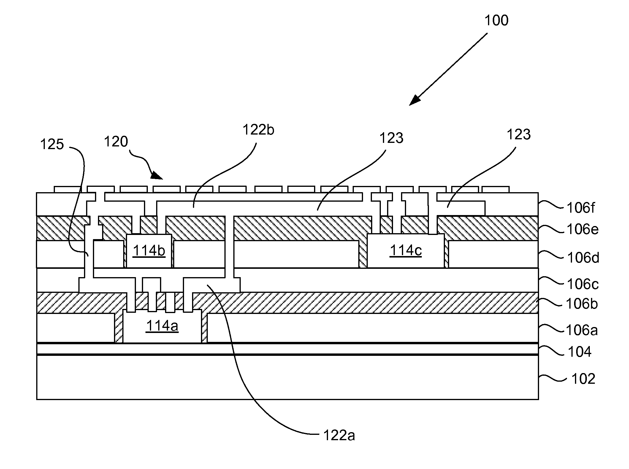
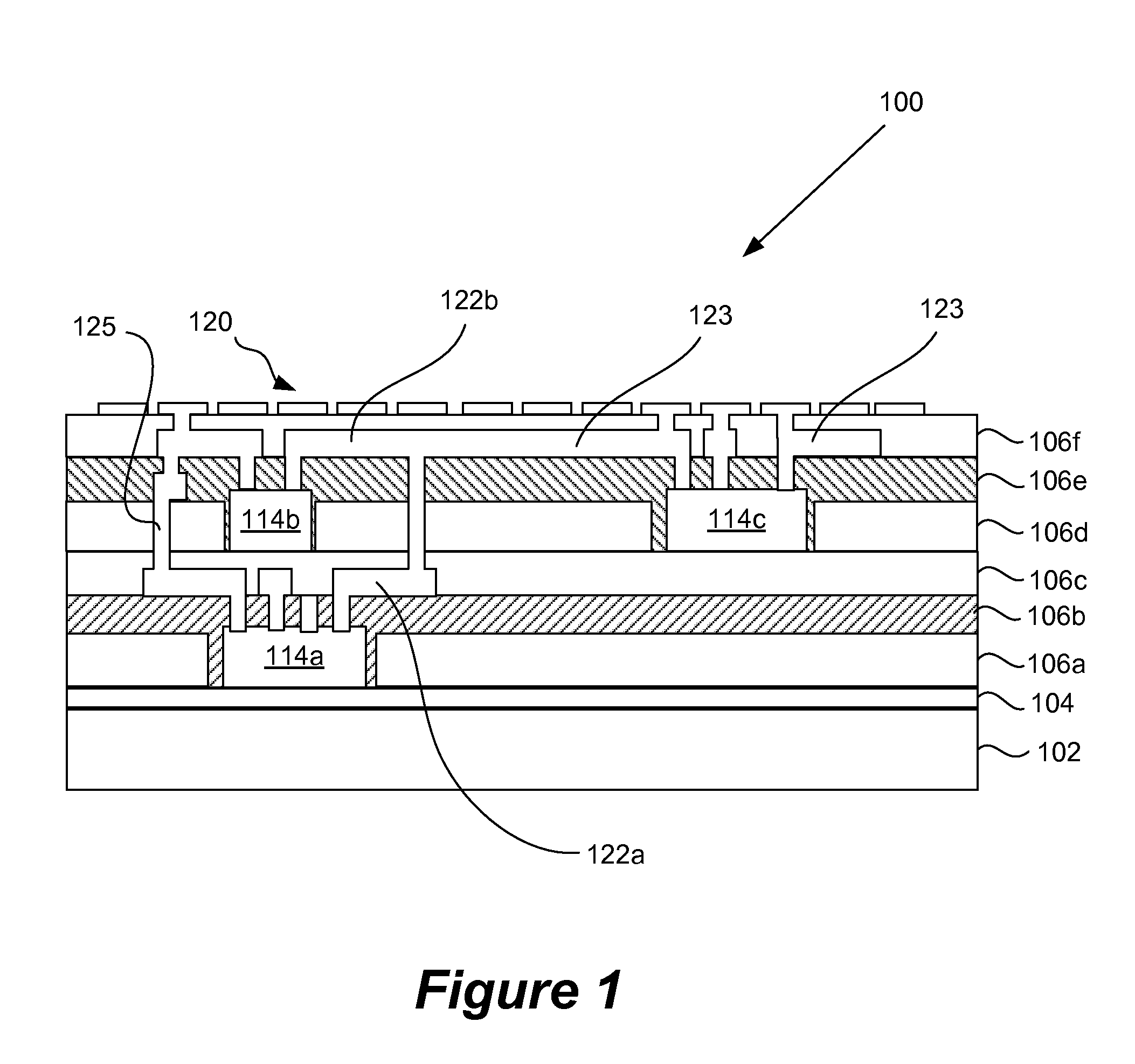
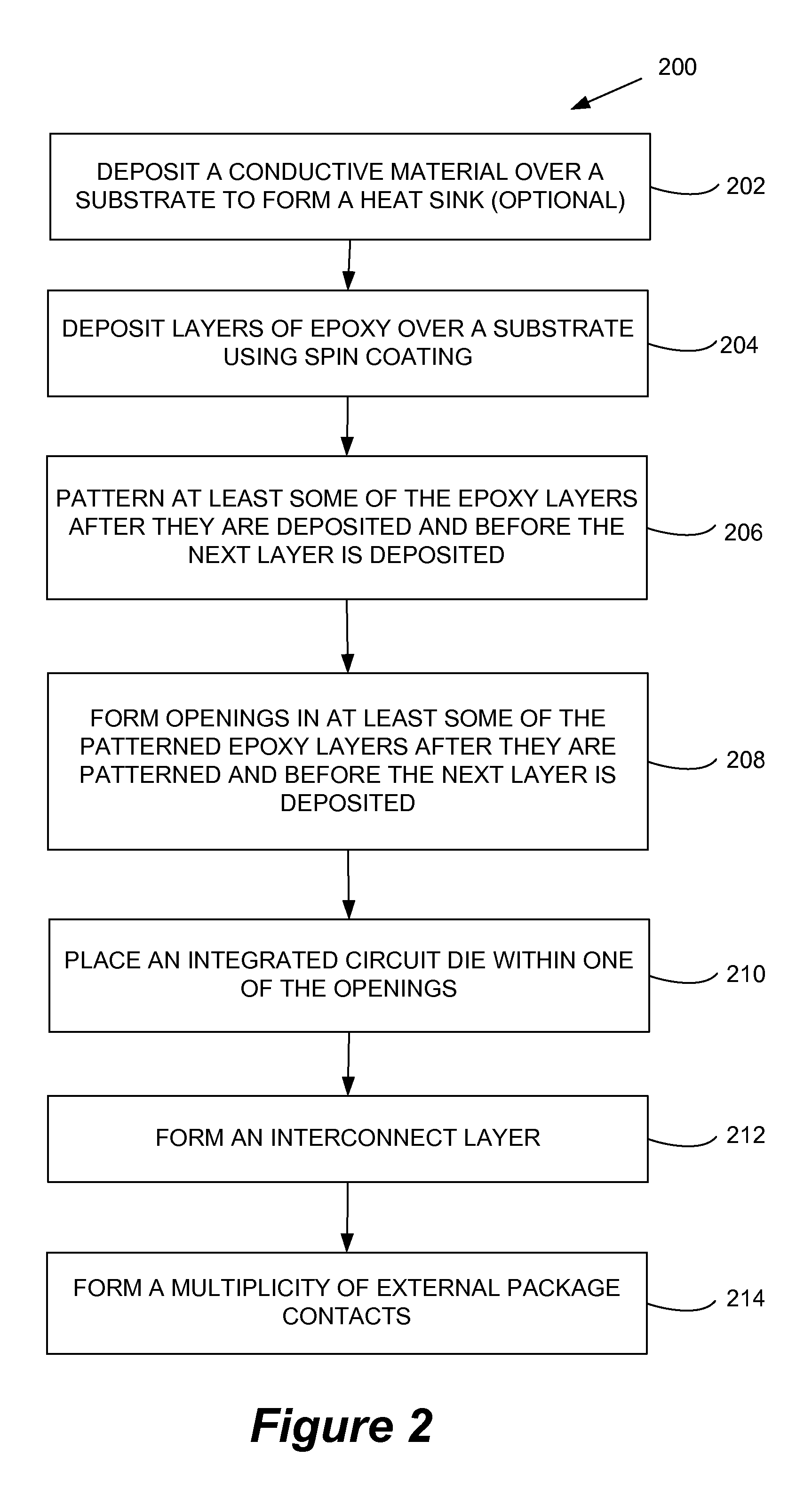
[0027]In one aspect, the present invention relates generally to integrated circuit (IC) packages and more specifically to IC micro-module technology. This aspect involves a micro-module made of multiple layers of a dielectric that is preferably photo-imageable and readily planarized. The micro-module may contain a variety of components including one or more integrated circuits, interconnect layers, heat sinks, conductive vias, passive devices, MEMS devices, sensors, thermal pipes etc. The various components can be arranged and stacked within the micro-module in a wide variety of different ways. The layers and components of the micro-module can be deposited and processed using various conventional wafer level processing techniques, such as spin coating, spray coating, lithography and / or electroplating. Another aspect of the present invention relates to wafer level manufacturing techniques and structures that integrate multiple active and / or passive components into a single, cost-effe...


PUM


Abstract

One aspect of the present invention relates to an integrated circuit package that includes multiple layers of a planarizing, photo-imageable epoxy that are formed over a substrate. In some designs, the substrate is a silicon wafer. An integrated circuit is embedded in the epoxy. An antenna, which is electrically coupled to the active face of the integrated circuit through an interconnect layer, is formed over one of the epoxy layers. In various embodiments, at least some of the epoxy layers are positioned between the substrate and the antenna such that there is a distance of at least approximately 100 microns between the substrate and the antenna.

Description

CROSS-REFERENCE TO RELATED APPLICATIONS[0001]This application is a Continuation-in-Part of and claims priority to U.S. patent application Ser. No. 12 / 643,924, entitled “Integrated Circuit Micro-Module,” filed Dec. 21, 2009, which in turn is a Continuation-in-Part and claims priority to U.S. Pat. No. 7,843,056, entitled “Integrated Circuit Micro-Module,” filed Feb. 20, 2009, both of which are hereby incorporated by reference in their entirety for all purposes.TECHNICAL FIELD[0002]The present invention relates generally to the packaging of integrated circuits (ICs). More particularly, the present invention relates to integrated circuit micro-modules.BACKGROUND OF THE INVENTION[0003]Portable electronics, such as cell phones, tablet computers, laptops and personal data assistants (PDAs) are increasingly popular. Currently, many portable electronics contain one or more antennae for wireless communications. The antennae are used to transmit and / or receive electromagnetic signals. There ar...

Claims


Application Information

Patent Timeline
IPC IPC(8): H01L23/50H01L21/50
CPCH01L21/4853H01L21/486H01L2924/1461H01L2924/07802H01L2224/73267H01L2224/32225H01L2924/014H01L2924/01087H01L2924/01033H01L2924/01024H01L2924/01006H01L2924/01005H05K2203/1469H01L21/568H01L21/6835H01L23/3114H01L23/3121H01L23/49816H01L23/49822H01L23/49827H01L23/5385H01L23/5389H01L23/66H01L24/24H01L24/82H01L24/97H01L25/0652H01L25/16H01L2221/68377H01L2223/6677H01L2224/24137H01L2224/24227H01L2224/2518H01L2224/97H01L2924/01003H01L2924/01013H01L2924/01015H01L2924/01029H01L2924/01074H01L2924/14H01L2924/15153H01L2924/15165H01L2924/1517H01L2924/15311H01L2924/19041H01L2924/19042H01L2924/19043H01L2924/3025H05K1/165H05K1/185H05K2201/10098H01L2224/82H01L2924/00
Inventor MOHAN, ANURAAGSMEYS, PETER
Owner NAT SEMICON CORP
Why Eureka
Try Eureka