Patterning Method of Metal Oxide Thin Film Using Nanoimprinting, and Manufacturing Method of Light Emitting Diode
Active Publication Date: 2011-07-14
KOREA INST OF MASCH & MATERIALS
View PDF6 Cites 27 Cited by
Summary
Abstract
Description
Claims
Application Information
AI Technical Summary
This helps you quickly interpret patents by identifying the three key elements:
Problems solved by technology
Method used
Benefits of technology
Benefits of technology
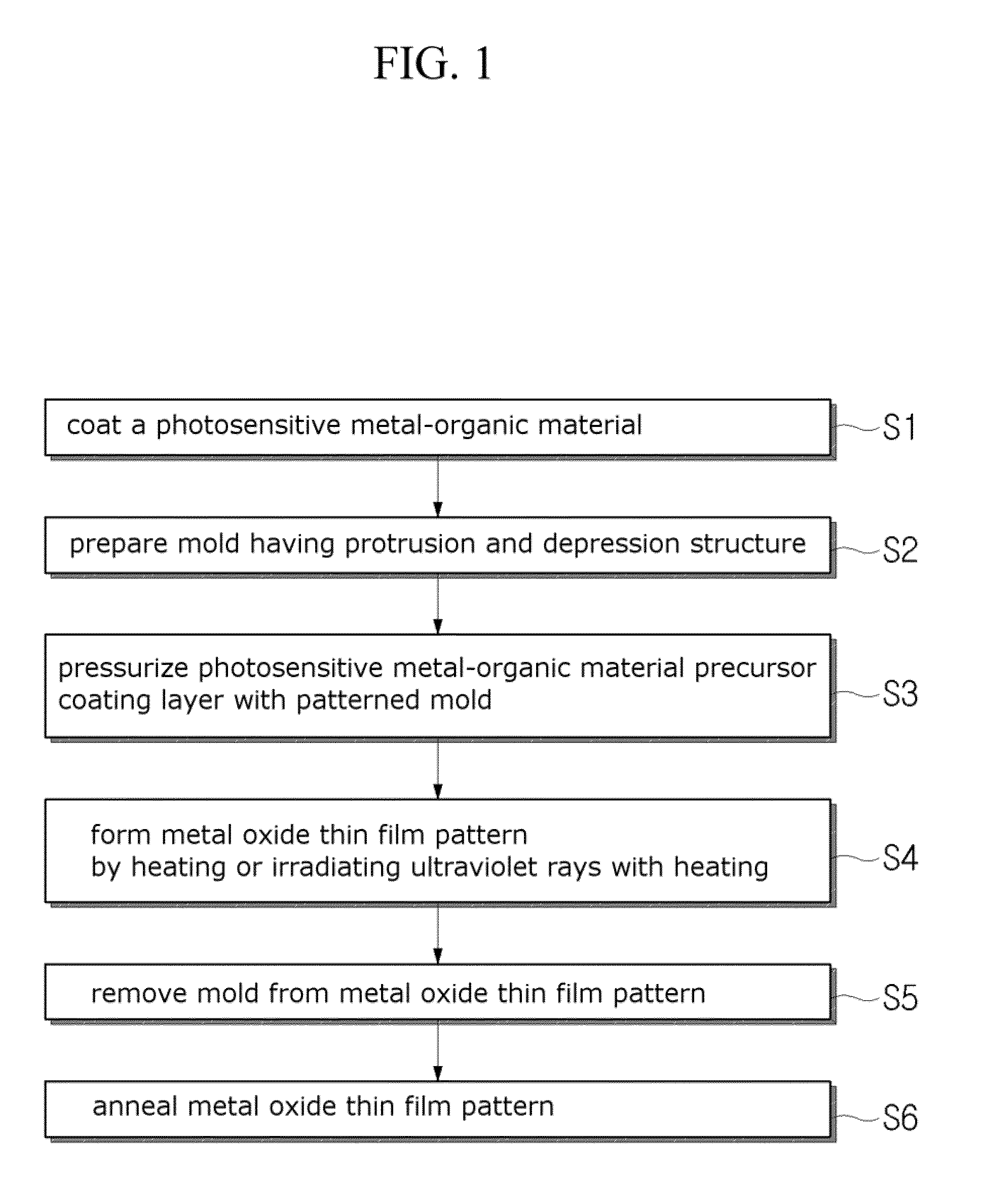
[0031]According to an exemplary embodiment of the present invention, there is provided a method for forming the metal oxide thin film pattern using the nanoimprinting, which makes it possible to simplify the process for forming the pattern since the process of separately applying the ultraviolet resin to be used as the resist can be omitted.
Problems solved by technology
When forming and patterning the metal oxide thin film on the substrate, the pattern is formed on the ultraviolet resin (resist) with the nanoimprint and the patterned metal oxide thin film is then formed by the etching process, such that the process is complicated.
Method used
Image
Click on the blue label to locate the original text in one second.
Reading with bidirectional positioning of images and text.
Examples
example 1
[0120]In order to compose the photosensitive metal-organic material precursor solution of titanium (Ti), 1.0000 g of a Ti(VI)(n-butoxide)2(2-ethylhexanoate)2 composition and 5.000 g of hexanes (Aldrich Colo., U.S.A.) are injected and mixed and agitated for 24 hours, thereby preparing a TiO2 sol of 0.27 molarity.
[0121]Herein, in order to compose Ti(VI)(n-butoxide)2(2-ethylhexanoate)2, 10.5266 g of Ti(VI)(n-butoxide)4 (Aldrich Colo., U.S.A.), 8.7400 g of 2-ethylhexanoic acid (Aldrich Colo., U.S.A.), and 15.000 g of hexanes are put in a round flask and evaporated and condensed by a rotary evaporator for 72 hours, thereby composing the Ti(VI)(n-butoxide)2(2-ethylhexanoate)2.
[0122]The photosensitive metal-organic material precursor solution of the composed titanium is spin-coated on one side of the upper end of the silicon substrate under a condition of 3000 rpm, and then the mold, in which a pattern in a pillar or line shape is formed, is pressed.
[0126]In order to compose the photosensitive metal-organic material precursor solution of tin (Sn), 1.0000 g of Sn(II)2-ethylhexanoate (Alfa Aesar Colo., U.S.A.) and 6.000 g of hexanes (Aldrich Colo., U.S.A.) are injected and mixed and agitated for 24 hours, thereby preparing a SnO2 sol of 0.21 molarity.
[0127]The photosensitive metal-organic material precursor solution of the composed tin (Sn) is spin-coated on one side of the upper end of the silicon substrate under a condition of 3000 rpm, and then the mold, in which the pattern in a pillar shape is formed, is pressed.
[0128]FIG. 10(a) shows a pattern formed by irradiating ultraviolet rays for 30 minutes, and FIG. 10(b) shows a pattern formed by heating for 7 minutes at a to temperature of 150°. Thereafter, the mold is released to form the SnO2 thin film pattern.
[0129]As shown in FIG. 10, it is confirmed that the SnO2thin film patterned by the ultraviolet or thermal nanoimprint process is formed by the nanoimprint process using the...
example 3
[0130]In order to compose the photosensitive metal-organic material precursor solution of various tins (Sn), 1.0000 g of Sn(II)2-ethylhexanoate (Alfa Aesar Colo., U.S.A.) and 6.000 g of MIBK(4-methyl-2-pentanone) (Aldrich Colo., U.S.A.) are injected and mixed and agitated for 24 hours, thereby preparing a SnO2(II) sol of 0.25 molarity.
[0131]The photosensitive metal-organic material precursor solution (II) of the composed tin (Sn) is spin-coated on one side of the upper end of the silicon substrate under a condition of 3000 rpm, and then the mold, in which the pattern in a pillar shape is formed, is pressed.
[0132]FIG. 11(a) shows a pattern formed by irradiating ultraviolet rays for 30 minutes, and FIG. 11(b) shows a pattern formed by heating for 7 minutes at a temperature of 150°. Thereafter, the mold is released to form the SnO2 thin film pattern.
[0133]As shown in FIG. 11, it is confirmed that the SnO2 thin film patterned is formed by the ultraviolet or thermal nanoimprint process u...
PUM
Property
Measurement
Unit
Temperature
aaaaa
aaaaa
Time
aaaaa
aaaaa
Time
aaaaa
aaaaa
Abstract
Disclosed are a patterning method of a metaloxide thin film using nanoimprinting, and a manufacturing method of a light emitting diode (LED). The method for forming a metaloxide thin film pattern using nanoimprinting includes: coating a photosensitive metal-organic material precursor solution on a substrate; preparing a mold patterned to have a protrusion and depression structure; pressurizing the photosensitive metal-organic material precursor coating layer with the patterned mold; forming a cured metal oxide thin film pattern by heating the pressurized photosensitive metal-organic material precursor coating layer or by irradiating ultraviolet rays to the pressurized photosensitive metal-organic material precursor coating layer while being heated; and removing the patterned mold from the metal oxide thin film pattern, and selectively further includes annealing the metal oxide thin film pattern. Within this, there is provided a method for forming a metal dioxe thin film pattern using nano imprinting, which makes it possible to simplify the process for forming the pattern since the process of separately applying the ultraviolet resin to be used as the resist can be omitted, and forms a micro / nano composite pattern through a single imprint process.
Description
CROSS-REFERENCE TO RELATED APPLICATION[0001]This application claims priority to and the benefit of Korean Patent Application No. 10-2010-0003109 filed in the Korean Intellectual Property Office on Jan. 13, 2010, the entire contents of which are incorporated herein by reference.BACKGROUND OF THE INVENTION[0002](a) Field of the Invention[0003]The present invention relates to a nanoimprint process, and more particularly, to a method for forming a metal oxide thin film pattern on a substrate using ultravioletirradiation or thermal nanoimprinting, and a manufacturing method of a light emitting diode (LED) device using the same.[0004](b) Description of the Related Art[0005]Nanoimprinting is a technology that proposes to realize nanoprocessing (1 to 100 nm) that is microprocessing, and involves transferring a pattern by applying pressure to a mold having a nanosize and that is applied with a photocurable resin or thermoplastic resin and irradiating ultraviolet rays to the mold or heating ...
Claims
Application Information
Patent Timeline
Application Date:The date an application was filed.
Publication Date:The date a patent or application was officially published.
First Publication Date:The earliest publication date of a patent with the same application number.
Issue Date:Publication date of the patent grant document.
PCT Entry Date:The Entry date of PCT National Phase.
Estimated Expiry Date:The statutory expiry date of a patent right according to the Patent Law, and it is the longest term of protection that the patent right can achieve without the termination of the patent right due to other reasons(Term extension factor has been taken into account ).
Invalid Date:Actual expiry date is based on effective date or publication date of legal transaction data of invalid patent.

