Coated light emitting device and method for coating thereof

a light-emitting device and light-emitting technology, applied in the direction of semiconductor/solid-state device manufacturing, semiconductor devices, electrical devices, etc., can solve the problems of stokes shift loss, efficiency loss, and severe loss of both material systems

Active Publication Date: 2011-07-21
LUMILEDS
View PDF12 Cites 90 Cited by
  • Summary
  • Abstract
  • Description
  • Claims
  • Application Information

AI Technical Summary

Benefits of technology

[0023]It is an object of the present invention to at least partly overcome these problems, and to provide a light emitting device and a method for producing such a light emitting device that does not suffer from loss of efficiency due to scattering of light through the lateral surfaces of the light emitting device.
[0039]The present inventors have realized that by using the method of the present invention to coat the lateral circumference surface, or lateral edge, of the light emitting device, a rapid and simple coating method can be achieved. The coating of the device may furthermore be achieved by using capillary force, to coat the lateral circumference surface. Due to this solid coating layer formed on the lateral circumference surface and the tuned optical properties of this coating, the light properties escaping the lateral edge of the light emitting device are controlled.
[0046]When these application methods are used, an exact amount of coating composition may be achieved. Thus, it is possible to control the amount of coating layer by controlling the amount of coating composition used.
[0057]Due to using different materials in the first and the second coating layer, it is possible to achieve different solid coating layers having reflective, diffusing, spectrally filtering, luminescent, and light blocking optical functionalities. Thus, the same lateral circumference surface may be coated by more than one coating layer having the same or different optical functionality.

Problems solved by technology

Both material systems suffer from severe losses in efficiency when their material composition is changed to shift the emission wavelength from blue towards green and from red towards green.
This color conversion comes with efficiency losses (mainly Stokes shift loss), but the high starting efficiency of blue LEDs makes even full-conversion to amber and red an attractive alternative to direct emitting AlInGaP systems that suffer from thermal efficiency issues.
This leads however to backscattering losses and processing variations.
However, this platelet phosphor technology requires a non-negligible thickness of the phosphor body compared to the size of the LED.
Still, the InGaN LED stack, consisting of quantum wells and anode, cathode and reflector, may have a thickness in the order of 10 μm and consist of materials with high refractive index, resulting in considerable waveguiding and non-negligible side emission.
The disadvantages relating to the light emitted from the lateral (edge) surfaces of a light emitting device are as follows:
For partial conversion Lumiramic, this may result in excess of blue light as well as significant variations of blue light flux present at large angles with respect to the normal direction and therefore reducing the over-angle color uniformity and consistency.
For full conversion Lumiramic, blue light leakage highly reduces the color purity of the green, amber or red LED.
In addition, this light leakage reduces the efficiency as part of the blue light is not converted to the desired color.
This is especially unwanted for full conversion phosphors, as incomplete conversion through the phosphor sides reduces color purity of the LED.
Generally, such light emitted towards the wrong side, as well as light emitted to the top direction but at large angles with the normal direction is hard to capture effectively in an optical system combined with the light source, such as collimator optics, lenses etc., and therefore is likely to reduce system efficiency.
The light scattered or reflected from the submount also increases the LED source area and results in stray light, which is undesired for etendue critical applications, such as automotive front lighting or projection LED systems.
In conclusion, the various embodiments of light emitting devices all suffer from disadvantages related to the side edges of the Lumiramic and / or the bonding layer and / or LED die.
These disadvantage are mainly related to color variations or limited color purity due to unwanted spectral differences between the side-emission and the top-emission.
Moreover, there will be a wavelength conversion light flux emission from the side surfaces partly (roughly by half) directed downward and sideward that is hard to use effectively in an application.
In addition, the etendue may also be increased compared to the active LED surfaces area, which is a disadvantage in etendue critical applications, such as projection LED systems, automotive headlamps or spot lights.
However, this method involves a specific coating apparatus, and is laborious and expensive.

Method used


Image

  • Coated light emitting device and method for coating thereof
  • Coated light emitting device and method for coating thereof
  • Coated light emitting device and method for coating thereof

Examples


embodiment 1

[0080]Many variations of embodiment 1 may be perceived. For example, full conversion or partial conversion phosphor top emitter may be used. For full conversion, the phosphor absorbs blue light and converts it to a large extent to another color with higher wavelength. The amount to which this occurs depends on the Lumiramic thickness and the concentration and absorption coefficients of the luminescence centers in the phosphor. It is strived to achieve sufficiently large path lengths in the phosphor to convert nearly all blue light to larger wavelengths such as green, amber or red. Due to the side coating, the over-angle color performance is very good, i.e. there is no blue light leak at larger angles.

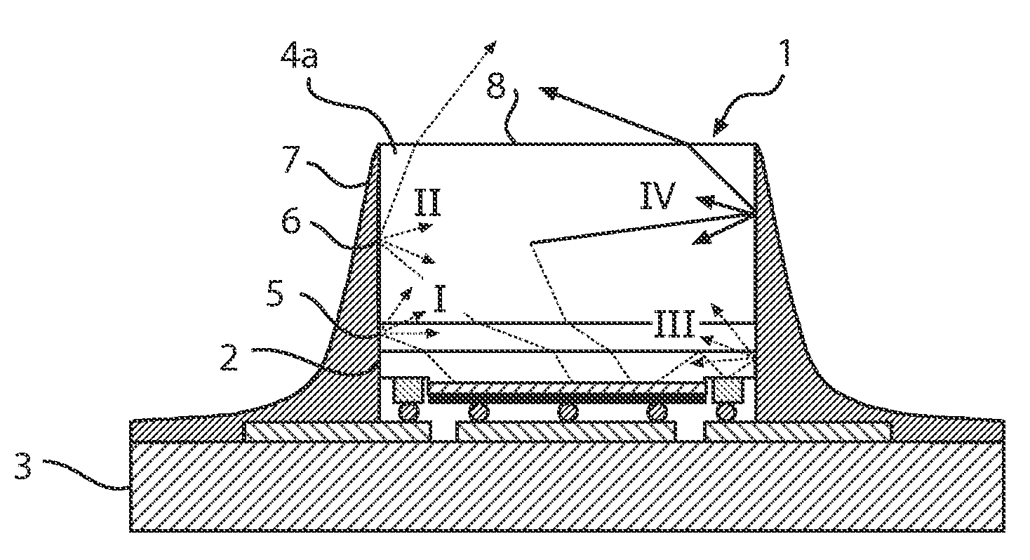
[0081]Another embodiment of the device of the present invention is illustrated in FIG. 2.

[0082]This embodiment is similar to embodiment 1, except that the side faces of the phosphor body 4a are angled, to have an overhang compared to the LED. Reflective coating is present on the right a...
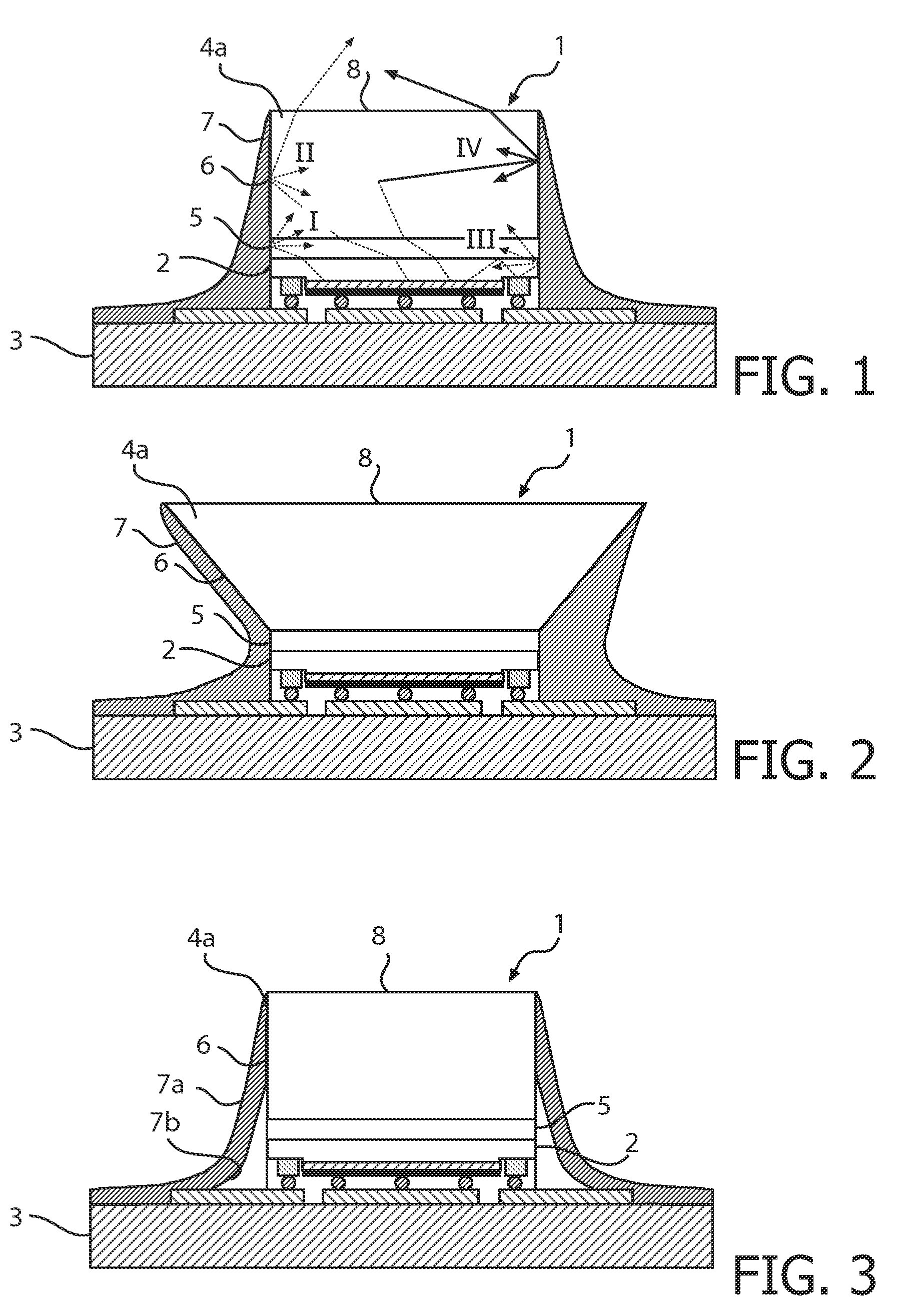
embodiment 5

[0103]In this embodiment of a side emitting light emitting device, similar to embodiment 5, a substrate is still present on the LED underneath the phosphor body. The coating layer is only present on the LED and substrate, not on the phosphor body.

[0104]As an alternative, the reflecting body may be arranged directly on the substrate. Coating may be present on the lateral surface of the substrate, without significant blue light leakage from the LED substrate side by using a reflective side coating. The phosphor may also extend beyond the LED substrate area (be oversized).

[0105]However, side emitting light emitting devices may also have other types of coating layers, such as diffusive or luminescent coating layers. By using a diffusive side-coating the angular and spectral distribution of the side-emission may be influenced, e.g. to make it more uniform.

[0106]By using a side coating that absorbs blue light and transmits converted light (e.g. amber light), a full conversion side emitter...


PUM


Abstract

The present invention relates to the field of a light emitting device (1), comprising a light emitting diode (2) arranged on a submount (3), said device having a lateral circumference surface (6) and a top surface (8), and an optically active coating layer (7), said coating layer (7):covering along at least a part of said circumference surface (6),extending from the submount (3) to said top surface (8), andessentially not covering the top surface (8). A method for producing the device is also disclosed.

Description

FIELD OF THE INVENTION[0001]The present invention relates to a light emitting device comprising a light emitting diode arranged on a submount, said device having a lateral circumference surface and a top surface, and an optically active coating layer. A method for applying such coating layer on a light emitting device is also disclosed.BACKGROUND OF THE INVENTION[0002]High power light emitting devices, containing light emitting diodes (LEDs), are used in an increasing number of illumination applications today. Generally, two material systems for making high-power LEDs are used.[0003]InGaN is used to produce efficient blue LEDs[0004]AlInGaP is used to produce efficient red and amber LEDs.[0005]Both material systems suffer from severe losses in efficiency when their material composition is changed to shift the emission wavelength from blue towards green and from red towards green.[0006]By application of wavelength converting materials, such as fluorescent and / or luminescent materials,...

Claims


Application Information

Patent Timeline
Patent Type & Authority Applications(United States)
IPC IPC(8): H01L33/44H01L27/15H01L33/46
CPCH01L33/44H01L33/46H01L2224/16225H01L33/54H01L25/0753H01L33/505H01L2224/05573H01L2224/05568H01L2924/00014H01L2224/0554H01L2224/05599H01L2224/0555H01L2224/0556
Inventor JAGT, HENDRIK J. B.KLEYNEN, CHRISTIANWEIJERS, ALDEGONDA L.
Owner LUMILEDS
Why Eureka
Try Eureka