

Semiconductor device
a technology of semiconductor devices and membranes, applied in the field of semiconductor devices, can solve the problems of reducing reliability, reducing the modulus and hardness of young, and removing the insulating film, so as to achieve the effect of easy moisture absorption, less moisture, and higher modulus and hardness
- Summary
- Abstract
- Description
- Claims
- Application Information
AI Technical Summary
Benefits of technology
Problems solved by technology
Method used
Image

Examples
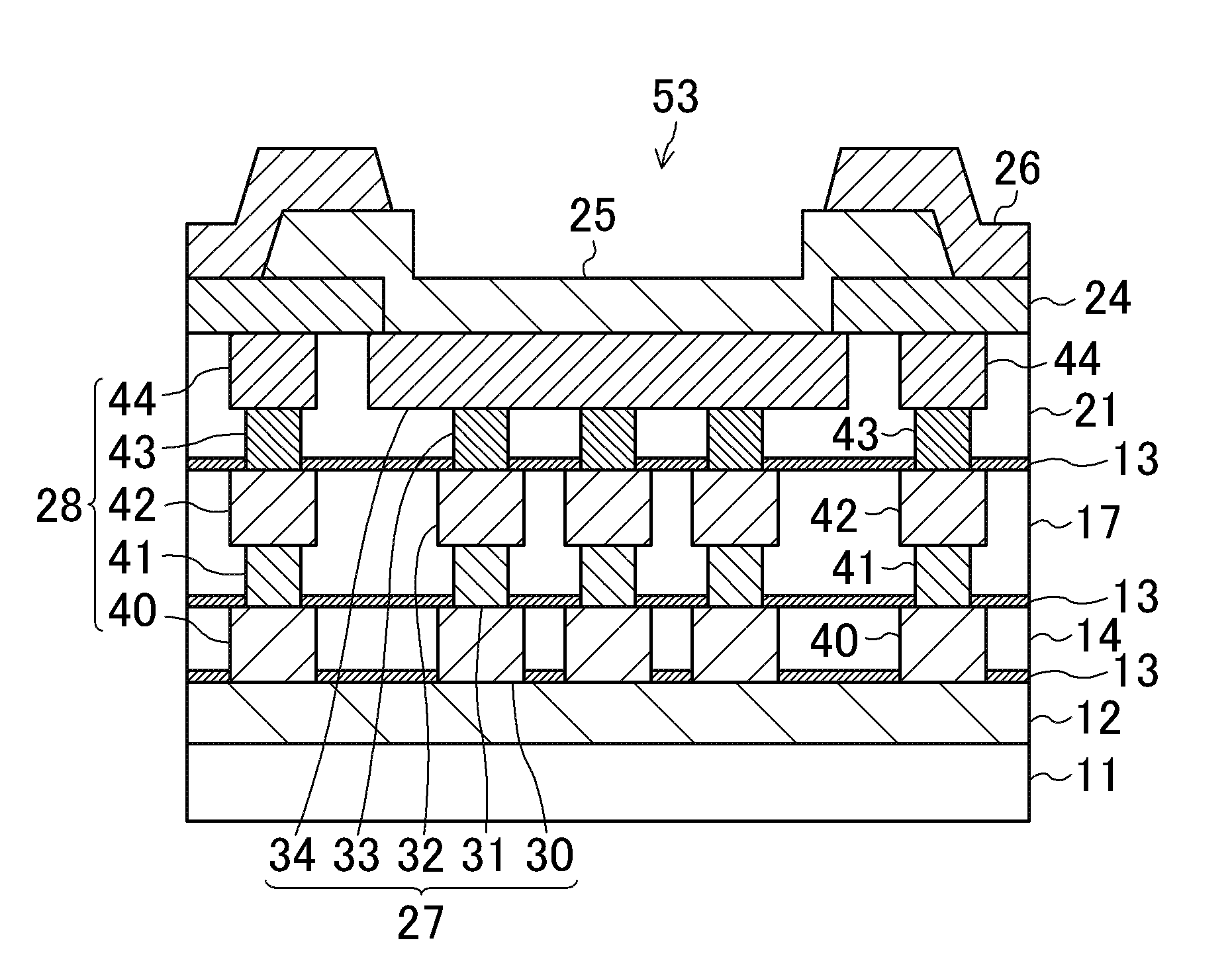
first example embodiment
Fifth Variation of First Example Embodiment
FIG. 14 illustrates an electrode pad structure in a semiconductor device according to a fifth variation of the first example embodiment.
As shown in FIG. 14, in the fifth variation, a fourth insulating film 21A located higher is made of silicon dioxide having a high dielectric constant in place of the low dielectric constant material.
As such, in this variation, the fourth insulating film 21A located higher, in which a crack is most easily caused by the external pressure applied to the electrode pad structure 53 and which easily absorbs moisture, is made of a material having higher Young's modulus and hardness, and absorbing less moisture than the material having a lower dielectric constant.
This increases the advantage of reducing the diffusion of the moisture and improving the mechanical strength in the electrode pad structure 53.
Second Example Embodiment
A semiconductor device according to a second example embodiment will be described herein...
second example embodiment
First Variation of Second Example Embodiment
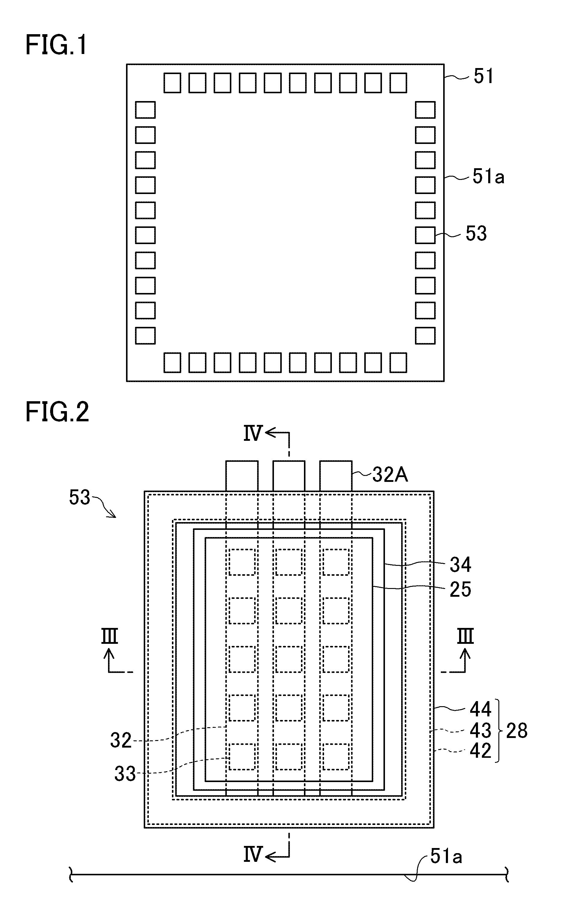
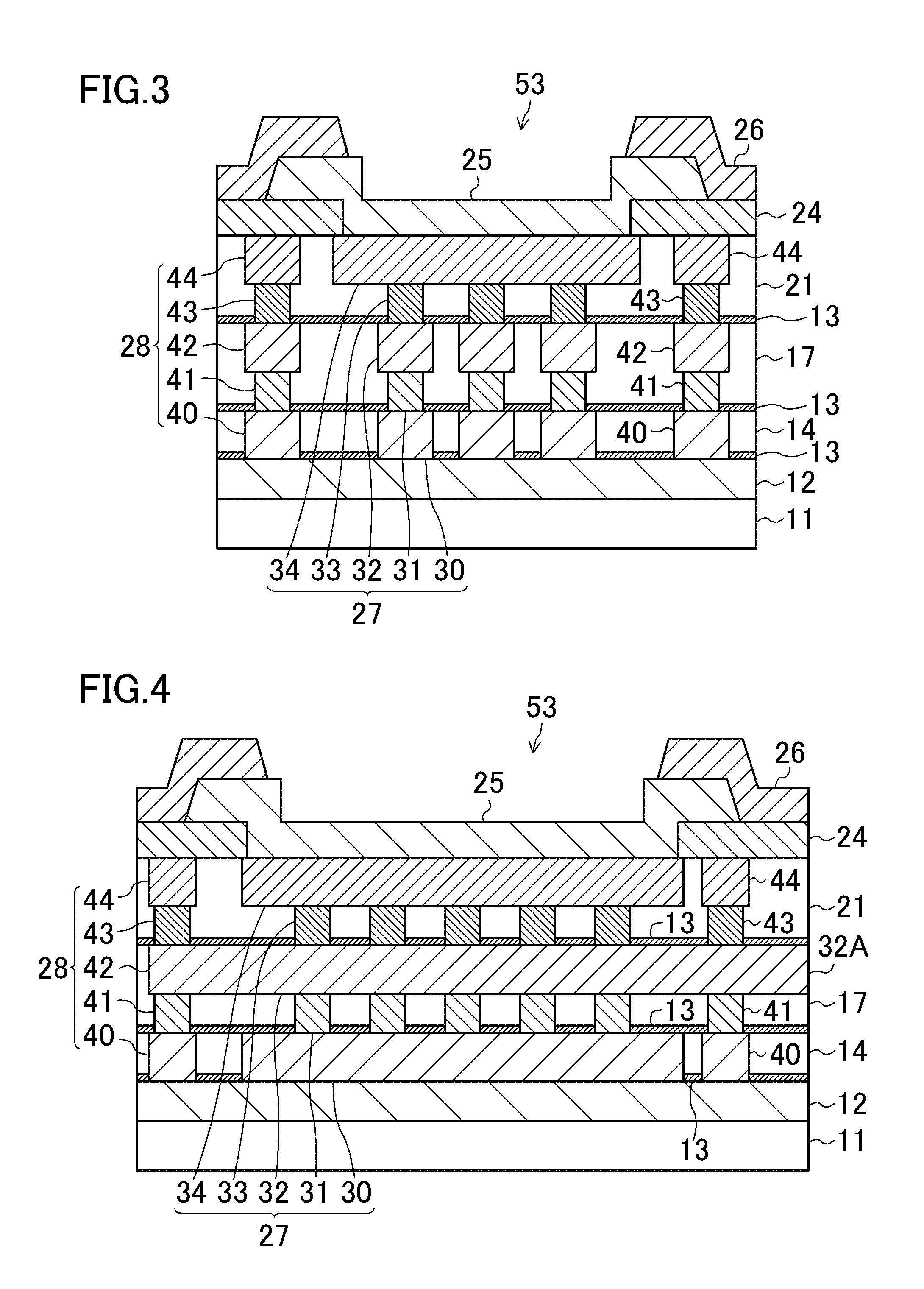
FIGS. 18-20 illustrate an electrode pad structure in a semiconductor according to a first variation of the second example embodiment.
As shown in FIGS. 19 and 20, in the first variation, two fine interconnects extending parallel to each other are used as the first interconnects 30 located lower in the multilayer 27. Similarly, two fine interconnects extending parallel to each other are used as the fourth interconnect 40 located lower in the ring body 28. That is, the number of the lower interconnects is larger than that of the higher interconnects.
In general, fine interconnects are needed in the internal circuit formed in the semiconductor chip 51. Thus, in the first variation, the plurality of fourth interconnects40 located lower in the ring body 28, which cannot have larger widths than the sixth interconnect 44 and the fifth interconnect 42 located higher, are used.
This structure reinforces the part of the interconnect of the ring body 28...
PUM
 Abstract
Description
Claims
Application Information