Photosensor device with dark current cancellation
- Summary
- Abstract
- Description
- Claims
- Application Information
AI Technical Summary
Benefits of technology
Problems solved by technology
Method used
Image
Examples
Embodiment Construction
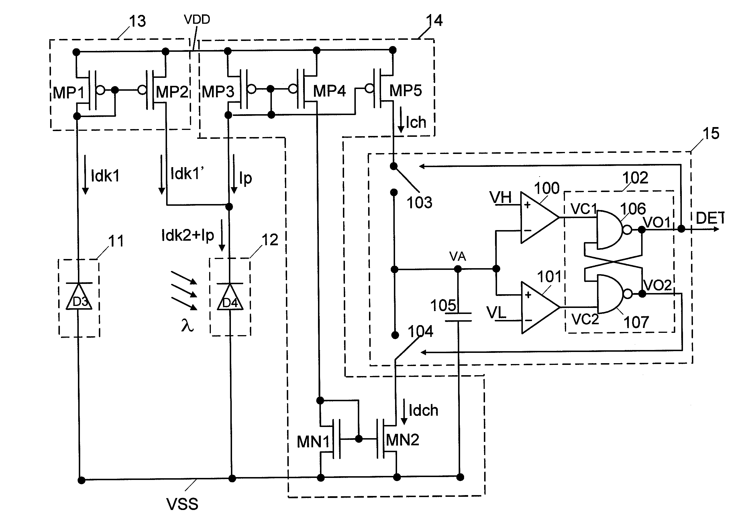
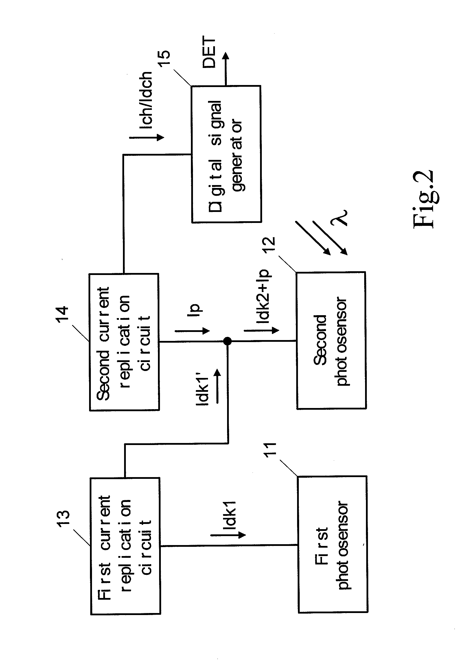
[0019]FIG. 2 is a block diagram of a photosensor device with dark current cancellation according to the preferred embodiment of the present invention. Refer to FIG. 2. The photosensor device comprises a first photosensor 11, a second photosensor 12, a first current replication circuit 13, a second current replication circuit 14 and a digital signal generator 15. The first photosensor 11 has a first dark current Idk1 but it does not receive any photo signal; the second photosensor 12 has a second dark current Idk2 and it receives a photo signal λ to generate a photocurrent Ip based on the photo signal λ. One terminal of the first current replication circuit 13 is connected to the first photosensor 11, and the other terminal is connected to the second photosensor 12. The replicated current Idk1′, which is generated according to the first dark current Idk1, injects into the second photosensor 12 for eliminating the second dark current Idk2, wherein the second dark current Idk2 is equal...
PUM
 Abstract
Description
Claims
Application Information


