Method for fabrication of a semiconductor device and structure

Inactive Publication Date: 2011-08-18
MONOLITHIC 3D
View PDF102 Cites 22 Cited by
  • Summary
  • Abstract
  • Description
  • Claims
  • Application Information

AI Technical Summary

Benefits of technology

[0020]Embodiments of the present invention seek to provide a new method for semiconductor device fabrication that may be highly desirable for custom products. Embodiments of the current invention suggest the use of a Re-programmable antifuse in conjunction with ‘Through Silicon Via’ to construct a new type of configurable logic, or as usually called, FPGA devices. Embodiments of the current invention may provide a solution to the challenge of high mask-set cost and low flexibility that exist

Problems solved by technology

Semiconductor manufacturing is known to improve device density in an exponential manner over time, but such improvements do come with a price.
The mask set cost required for each new process technology has been increasing exponentially.
These changes represent an increasing challenge primarily to custom products, which tend to target smaller volume and less diverse markets therefore making the increased cost of product development very hard to accommodate.
Yet, it is always a challenge to come up with minimum set of Master Slices that will provide a good fit for the maximal number of designs because it is quite costly if a dedicated mask set is required for each Master Slice.
The difficulty to provide variable-sized array structure devices is due to the need of providing I/O cells and associated pads to connect the device to the package.
This method places a severe limitation on the I/O cell to use the same type of transistors as used for the logic an

Method used


Image

  • Method for fabrication of a semiconductor device and structure
  • Method for fabrication of a semiconductor device and structure
  • Method for fabrication of a semiconductor device and structure

Examples


Embodiment Construction

[0109]Embodiments of the present invention are now described with reference to FIGS. 1-13, it being appreciated that the figures illustrate the subject matter not to scale or to measure.

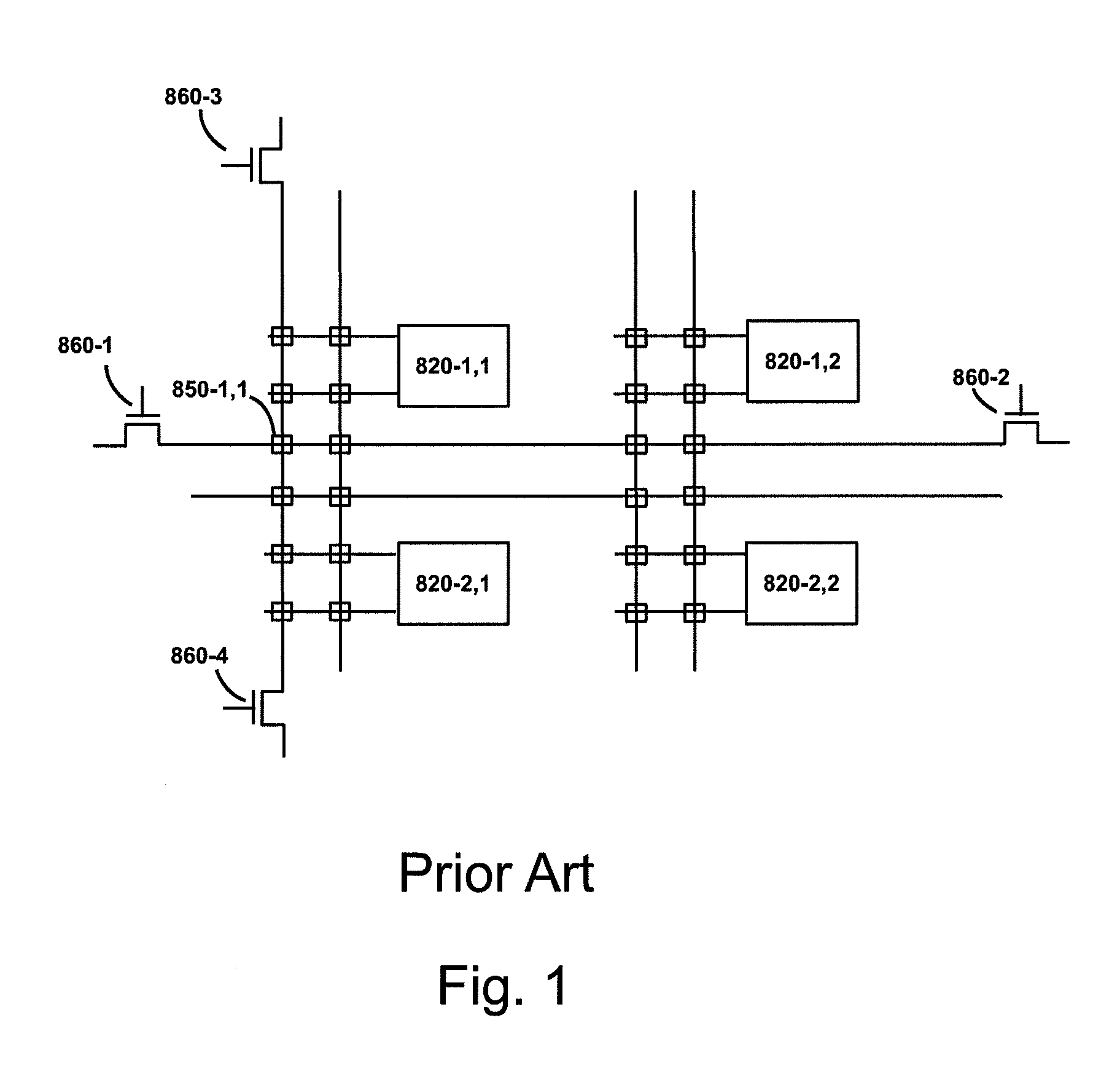
[0110]FIG. 1 illustrates a circuit diagram illustration of a prior art, where, for example, 860-1 to 860-4 are the programming transistors to program antifuse 850-1,1.

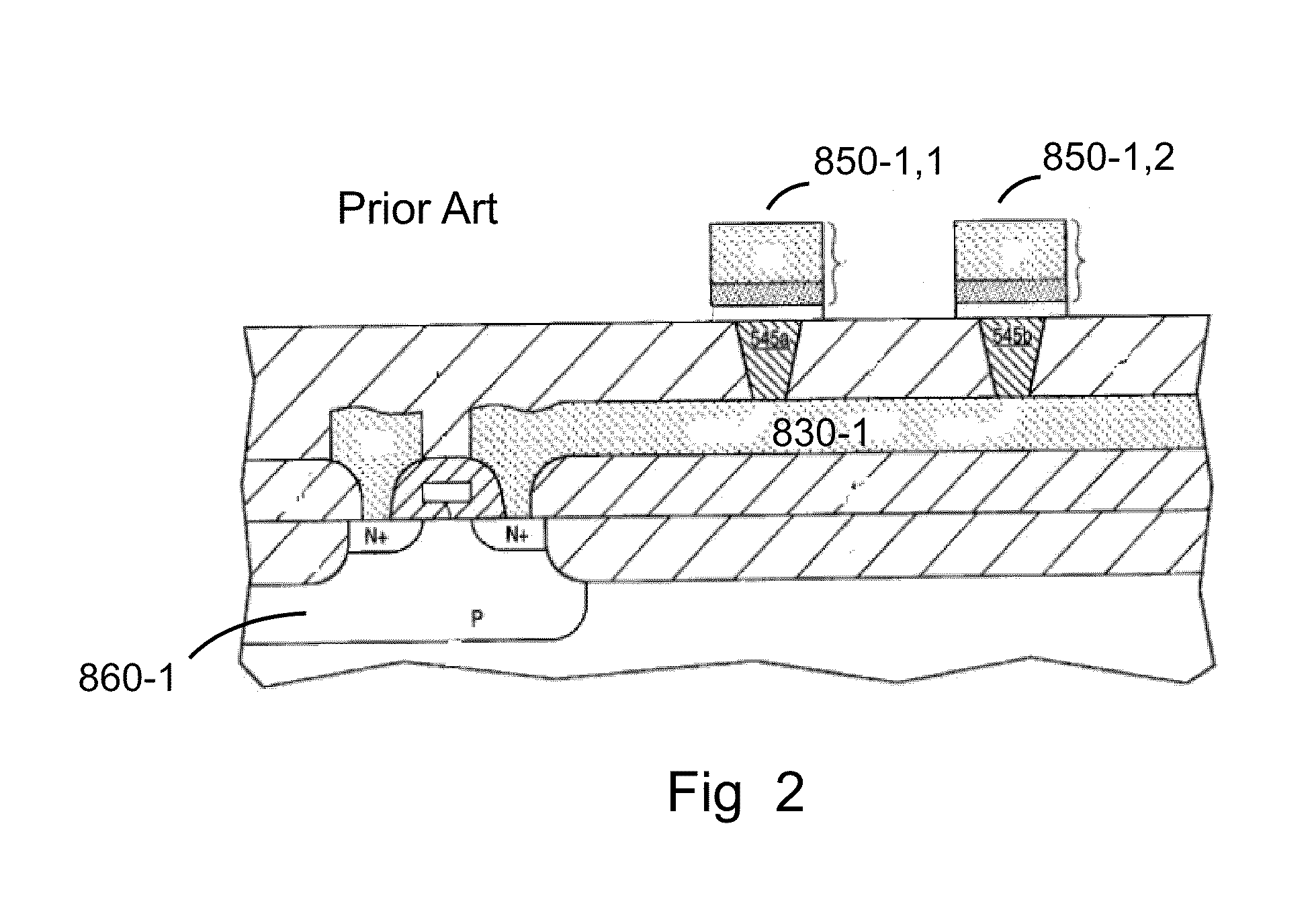
[0111]FIG. 2 is a cross-section illustration of a portion of a prior art represented by the circuit diagram of FIG. 1 showing the programming transistor 860-1 built as part of the silicon substrate.

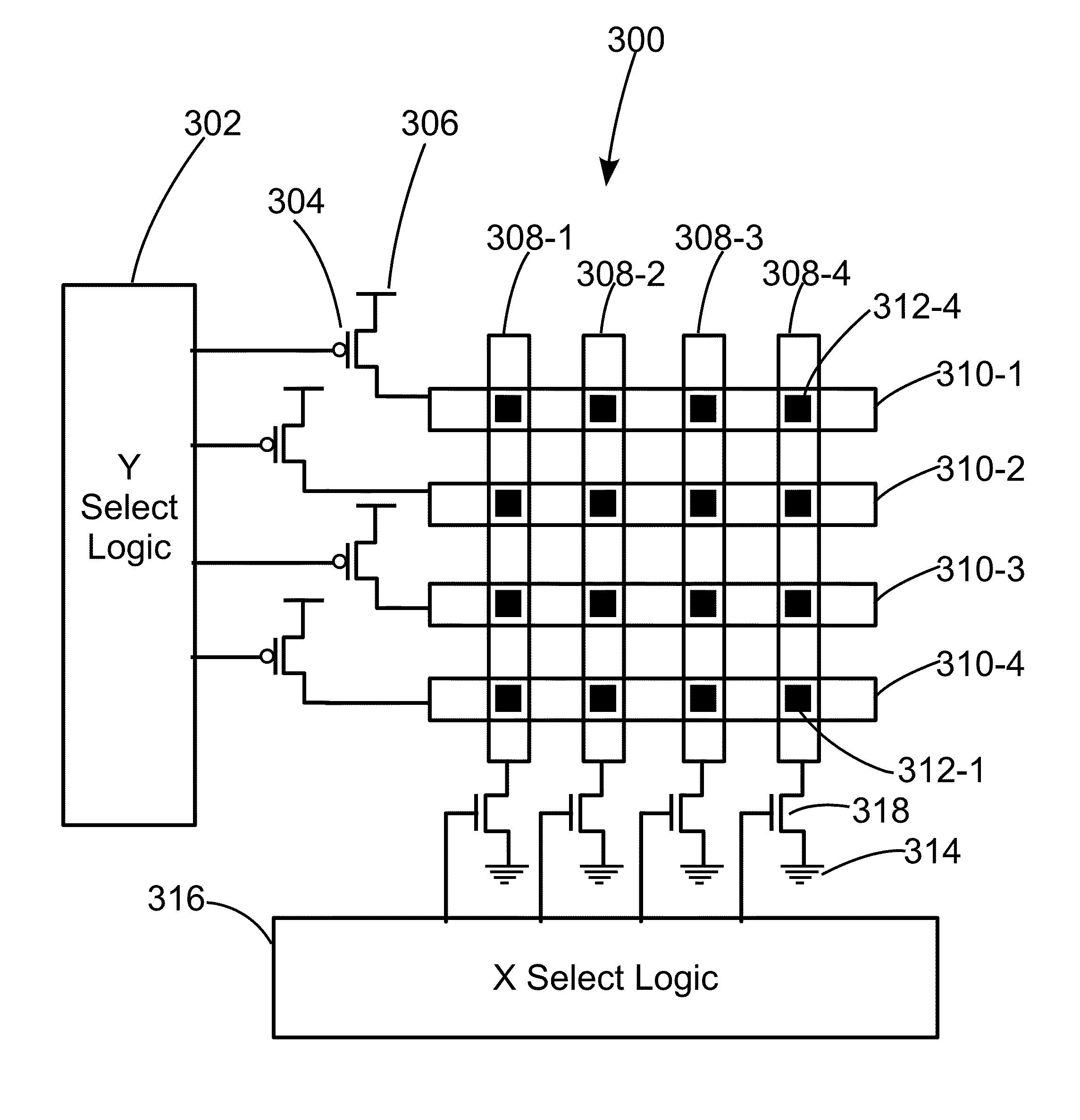
[0112]FIG. 3A is a drawing illustration of a programmable interconnect tile. 310-1 is one of 4 horizontal metal strips, which form a band of strips. The typical IC today has many metal layers. In a typical programmable device the first two or three metal layers will be used to construct the logic elements. On top of them metal 4 to metal 7 will be used to construct the interconnection of those logic elements. In an FPGA device the logic eleme...


PUM


Abstract

A Configurable device comprising, a logic die connected by at least one through silicon-via (TSV), to an input/output (I/O) die.

Description

CROSS-REFERENCE OF RELATED APPLICATION[0001]This application is related to U.S. patent application Ser. Nos. 12 / 577,532 and 12 / 423,214.BACKGROUND OF THE INVENTION[0002]1. Field of the Invention[0003]Various embodiments of the present invention may relate to configurable logic arrays and / or fabrication methods for a Field Programmable Logic Array—FPGA.[0004]2. Discussion of Background Art[0005]Semiconductor manufacturing is known to improve device density in an exponential manner over time, but such improvements do come with a price. The mask set cost required for each new process technology has been increasing exponentially. So while 20 years ago a mask set cost less than $20,000 it is now quite common to be charged more than $1M for today's state of the art device mask set.[0006]These changes represent an increasing challenge primarily to custom products, which tend to target smaller volume and less diverse markets therefore making the increased cost of product development very har...

Claims


Application Information

Patent Timeline
IPC IPC(8): H03K19/173H01L23/538H01L21/306H01L21/26H01L21/70
CPCH01L21/76232H01L2924/10253H01L21/8221H01L21/84H01L23/481H01L23/49827H01L24/16H01L24/48H01L25/0657H01L25/18H01L25/50H01L27/0207H01L27/0688H01L27/1203H01L2224/13025H01L2224/131H01L2224/16225H01L2224/17181H01L2224/48145H01L2225/06506H01L2225/06513H01L2225/06517H01L2225/06541H01L2924/1431H01L2924/1434H01L2924/1436H01L2924/1443H01L2924/15311H01L2924/3011H01L21/76254H01L2924/1305H01L2924/01019H01L2924/01066H01L2924/01322H01L2924/13091H01L2924/13062H01L2924/1301H01L2924/00013H01L2924/014H01L2224/13099H01L2224/13599H01L2224/05599H01L2224/05099H01L2224/29099H01L2224/29599H01L2924/00H01L2924/00014H01L2924/12032H01L2924/14H01L2224/45099H01L2224/45015H01L2924/207H01L2924/00012
Inventor OR-BACH, ZVICRONQUIST, BRIANWURMAN, ZEEVBEINGLASS, ISRAELDE JONG, J. L.
Owner MONOLITHIC 3D
Why Eureka
Try Eureka