Substrate processing method

a processing method and substrate technology, applied in the direction of photomechanical equipment, instruments, cleaning using liquids, etc., can solve the problems of insufficient ultra-miniaturized semiconductor devices, non-uniform line insufficient line width of second resist patterns, so as to reduce non-uniform line widths and reduce productivity

Active Publication Date: 2011-08-18
TOKYO ELECTRON LTD
View PDF1 Cites 1 Cited by
  • Summary
  • Abstract
  • Description
  • Claims
  • Application Information

AI Technical Summary

Benefits of technology

[0015]In accordance with the present disclosure, when resist patterns are formed by performing double patterning such as a LLE process, it is possible to reduce non-uniformity in line widths of a second resist pattern on a wafer without lowering productivity.

Problems solved by technology

For this reason, conventionally, light of a shorter wavelength has been used for an exposure process, but it is not sufficient for an ultra-miniaturized semiconductor device after 45 nm node.
However, if resist patterns are formed by performing double patterning such as the above-described LLE process, there is a following problem.
However, if the cleaning process is not performed sufficiently, there may occur a development failure in the development process of the second patterning process, which may result in non-uniformity in line widths of the second resist pattern.
Particularly, the line widths of the second resist pattern are not uniform between a central area of the wafer and a periphery area of the wafer.
However, the sufficiently long time for the cleaning process may increase a time for processing a single sheet of a wafer, i.e., a so-called “tact time”, and, thus, the number of processed wafers per unit time may decrease and productivity may be lowered.

Method used


Image

  • Substrate processing method
  • Substrate processing method
  • Substrate processing method

Examples


first embodiment

[0049]Above all, a substrate processing method and a substrate processing system employing the substrate processing method in accordance with a first embodiment will be explained with reference to FIGS. 1 to 14.

[0050]Referring to FIGS. 1 and 2, a substrate processing system in accordance with the present embodiment will be explained. In this substrate processing system, a coating / developing apparatus is connected with an exposure apparatus.

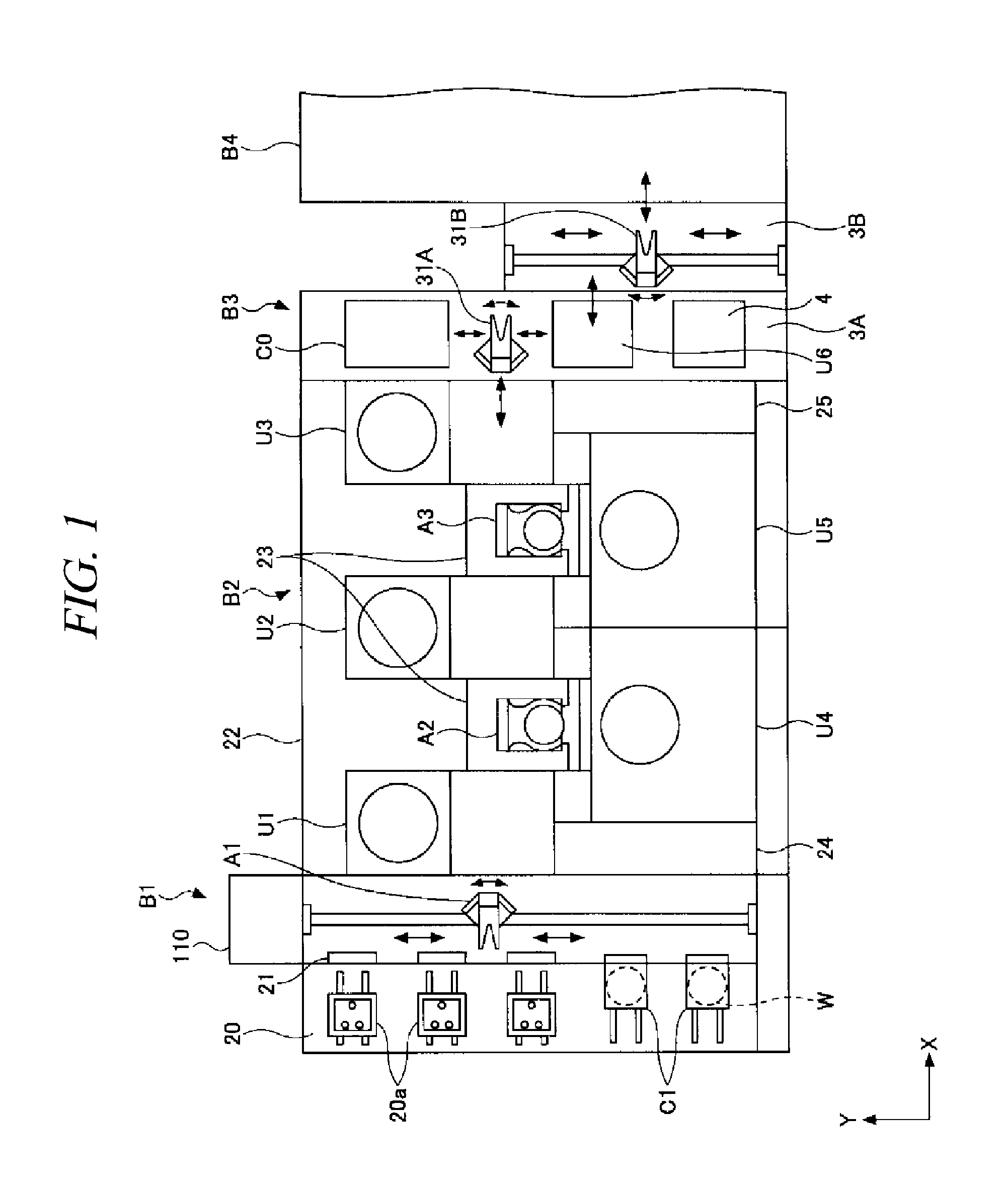
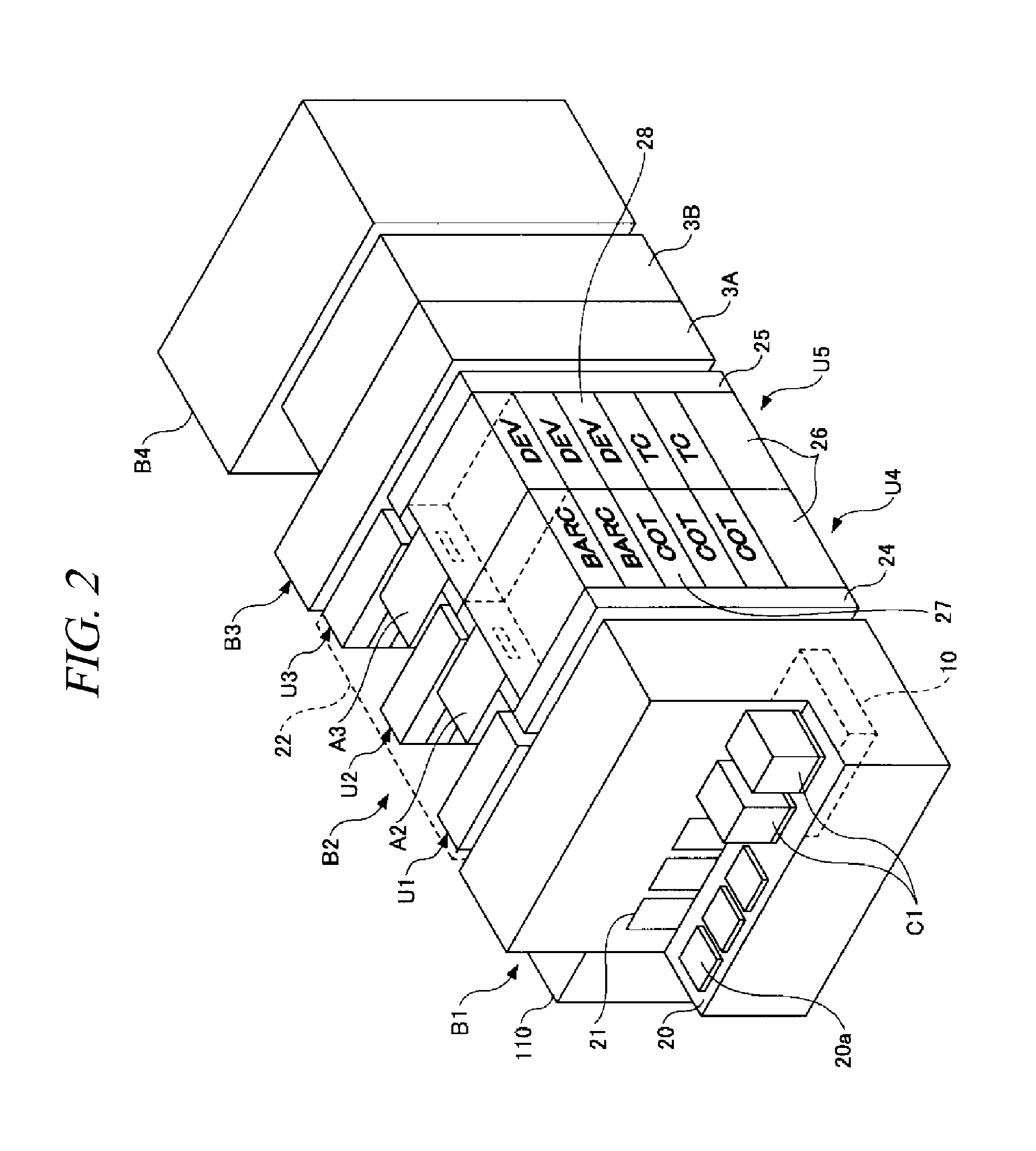
[0051]FIG. 1 is a plane view showing a schematic configuration of a substrate processing system in accordance with the present embodiment, and FIG. 2 is a perspective view showing a schematic configuration of the substrate processing system in accordance with the present embodiment.

[0052]The substrate processing system includes a carrier mounting unit B1, a processing unit B2, an interface unit B3, and an exposure unit B4.

[0053]The carrier mounting unit B1 includes a carrier station 20, an opening / closing unit, and a transit mechanism A1. The carr...

first modification example of first embodiment

[0170]Hereinafter, referring to FIGS. 17 and 18, there will be explained a substrate processing method in accordance with a first modification example of the first embodiment.

[0171]A substrate processing method of the present modification example is different from the substrate processing method in accordance with the first embodiment in that a processing time t is determined based on a relationship between the processing time t and line widths CD2-1 and CD2-2 of a second resist pattern P2 on both a central area of a wafer W and a periphery area of the wafer W.

[0172]In this modification example, the substrate processing system, the developing unit, and the line width measurement apparatus explained in the first embodiment may be used.

[0173]FIG. 17 is a flow chart for explaining a sequence of processes of a substrate processing method in accordance with the present modification example. FIG. 18 is a graph schematically showing a relationship between a processing time and a space widt...

second modification example of first embodiment

[0188]Hereinafter, referring to FIGS. 19 to 22, there will be explained a substrate processing method in accordance with a second modification example of the first embodiment.

[0189]The substrate processing method in accordance with the present modification example is different from the substrate processing method of the first embodiment in that first data include a first processing condition under which a cleaning process is performed on the wafer W in the first process and the first data show a relationship between a condition other than a processing time and a line width CD2 of a second resist pattern P2.

[0190]In the present modification example, the substrate processing system, the developing unit, and the line width measurement apparatus explained in the first embodiment may be used.

[0191]FIG. 19 is a flow chart for explaining a sequence of processes of the substrate processing method in accordance with the present modification example.

[0192]As depicted in FIG. 19, the substrate...


PUM

PropertyMeasurementUnit
wavelengthaaaaaaaaaa
space width SP1aaaaaaaaaa

Abstract

A substrate processing method includes a first process (step S12 to step S16) of forming a first resist pattern by exposing a substrate having thereon a first resist film to lights, developing the exposed substrate and cleaning the developed substrate; and a second process (step S17 to step S20) of forming a second resist pattern by forming a second resist film on the substrate having thereon the first resist pattern, exposing the substrate having thereon the second resist film to lights, and developing the exposed substrate. A first processing condition is determined based on first data showing a relationship between a first processing condition under which a cleaning process is performed on the substrate in the first process (step S16) and a line width of the second resist pattern, and the first process (step S16) is performed on the substrate under the determined first processing condition.

Description

CROSS-REFERENCE TO RELATED APPLICATION[0001]This application claims the benefit of Japanese Patent Application Nos. 2010-029339 and 2010-266897 filed on Feb. 12, 2010 and Nov. 30, 2010, respectively, the entire disclosures of which are incorporated herein by reference.FIELD OF THE INVENTION[0002]The present disclosure relates to a substrate processing method for processing a substrate.BACKGROUND OF THE INVENTION[0003]In manufacturing a semiconductor device, there has been used photolithography as a patterning technique for forming a circuit pattern on a semiconductor wafer (hereinafter, simply referred to as “wafer”) as a processing target substrate. In order to form the circuit pattern by using photolithography, a resist film is formed on a wafer by coating the wafer with a resist solution, the resist film is exposed to lights irradiated onto the resist film so as to correspond to the circuit pattern, and then the exposed resist film is developed.[0004]Recently, as a semiconductor ...

Claims


Application Information

Patent Timeline
Patent Type & Authority Applications(United States)
IPC IPC(8): G03F7/20
CPCG03F7/0035G03F7/2041H01L21/6715H01L21/0206H01L21/0273G03F7/40
Inventor NAKAMURA, HIROSHINIWA, TAKAFUMIKUWAHARA, YUHEITOMITA, TADATOSHI
Owner TOKYO ELECTRON LTD
Why Eureka
Try Eureka