Method for integrating an electronic component into a printed circuit board

a technology of electronic components and printed circuit boards, applied in the association of printed circuit non-printed electric components, printed circuit aspects, lithographic masks, etc., can solve problems such as the inability to connect individual layers, and achieve the effects of avoiding damage to already fixed components, simple and reliable production, and large process tolerances

Active Publication Date: 2011-08-25
AT & S AUSTRIA TECH & SYSTTECHN AG
View PDF21 Cites 14 Cited by
  • Summary
  • Abstract
  • Description
  • Claims
  • Application Information

AI Technical Summary

Benefits of technology

[0026]In addition to the simple and reliable production of holes or perforations corresponding to the contacts of the already fixed component, it is proposed according to a further preferred embodiment that, in addition to forming holes or perforations corresponding to the contacts of the component, in the conducting layer and in the non-conducting layer, at least one further perforation is formed outside the region of the fixation of the component to the laminate in order to provide an additional perforation for the formation of a subsequent feedthrough and/or for the formation of the contour of a circuit board element. Due to such a formation of at least one further perforation outside the region of the fixation of the component, and hence the contacts of the same, in particular for the formation of a subsequent feedthrough, it has become possible to provide or realize such a perforation or bore much more closely to the fixed component. Such an additional perforation will thus not have to be formed in a subsequent or independent method step, for instance as a mechanical bore at the end of the overall production process of the circuit board, wherein, by the subsequent or independent formation of such an additional bore, significantly larger process tolerances will have to be observed, in particular, to avoid damage to the already fixed component. When using the at least one additional or further perforation to produce the contour of a circuit board element or printed circuit board corresponding to the contour of a finished circuit board or a circuit board to be produced, it will, moreover, be possible, similarly as in the formation of a subsequent feedthrough, to renounce subsequent mechanical separation processes like milling to produce the contour of a circuit board. A common method or process step will thus also make possible to simultaneously form the contour of the circuit board to be produced, corresponding to the edges of the circuit board, closer to the component to be fixed due to smaller process tolerances, thus miniaturizing the same. The use of, for instance, a laser drilling procedure or laser technology for making the further perforation to form a feedthrough and/or the contour of the circuit board will, in the main, enable a more precise configuration of such additional perforations as opposed to mechanical processing procedures. Furthermore, registering and aligning will, in particular, be improved in that all holes or perforations both for contacting the component by exposing the contacts and for producing additional perforations will be realized in a common working step while jointly aligning and registering. By forming at least one further perforation during, or along with, the formation of holes or perforations in the conducting layer and subsequently also in the insulating layer, it has thus become possible to promote the usually sought miniaturization of a circuit board to be produced, by reducing the mutual distances of individual elements or such a feedthrough or the contour of the circuit board to be produced, of an integrated component. The available surface will thus be significantly better utilized.
[0027]To further simplify the production procedure and to increase the accuracy of, in particular, the arrangement of the additional or further perforation, it is proposed according to a further preferre

Problems solved by technology

Thus, in particular, no air or gas inclusions whatsoever will be present in at least some layers as opposed to the known prior art, which may lead to improper connections of individual layers during such a pressing or laminating

Method used


Image

  • Method for integrating an electronic component into a printed circuit board
  • Method for integrating an electronic component into a printed circuit board
  • Method for integrating an electronic component into a printed circuit board

Examples


example 1

[0055]Thin insulating layer (15-30 μm) and / or adhesive with low filler content

[0056]Pulsed CO2 laser

[0057]Power: 3 watts

[0058]Beam diameter: 180 μm

[0059]Pulse duration: 6 μs

[0060]Number of pulses: 13

[0061]Hole diameter: 75 μm

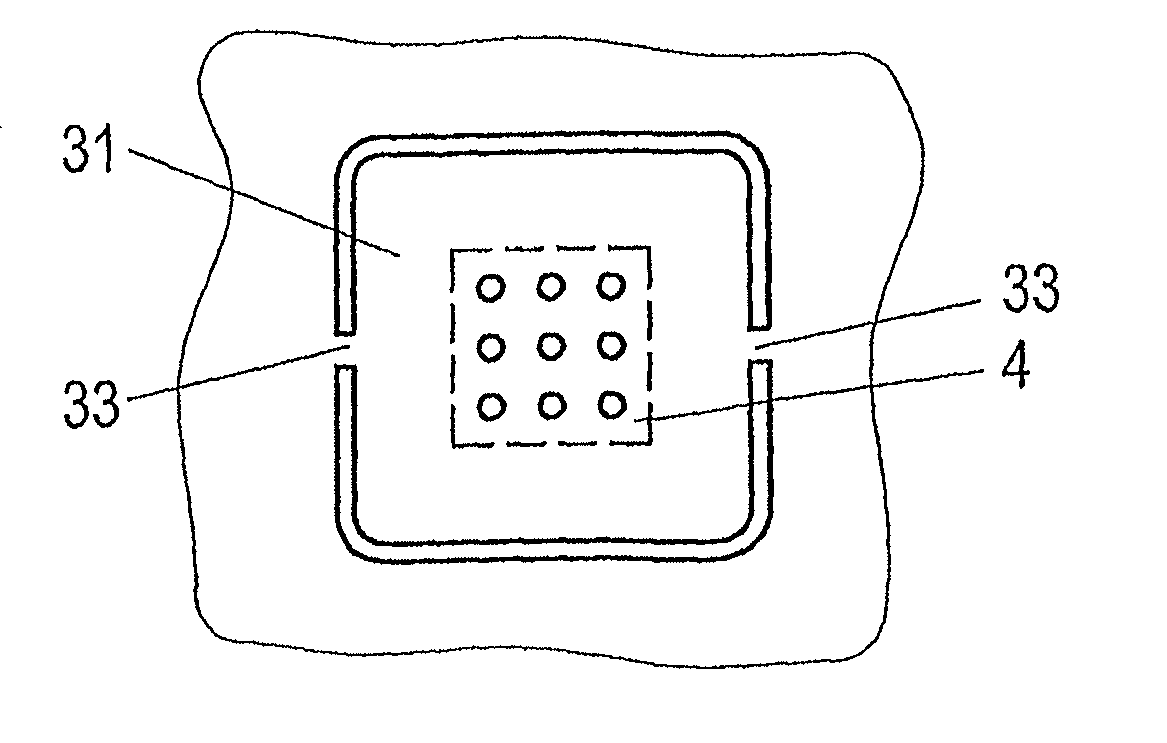
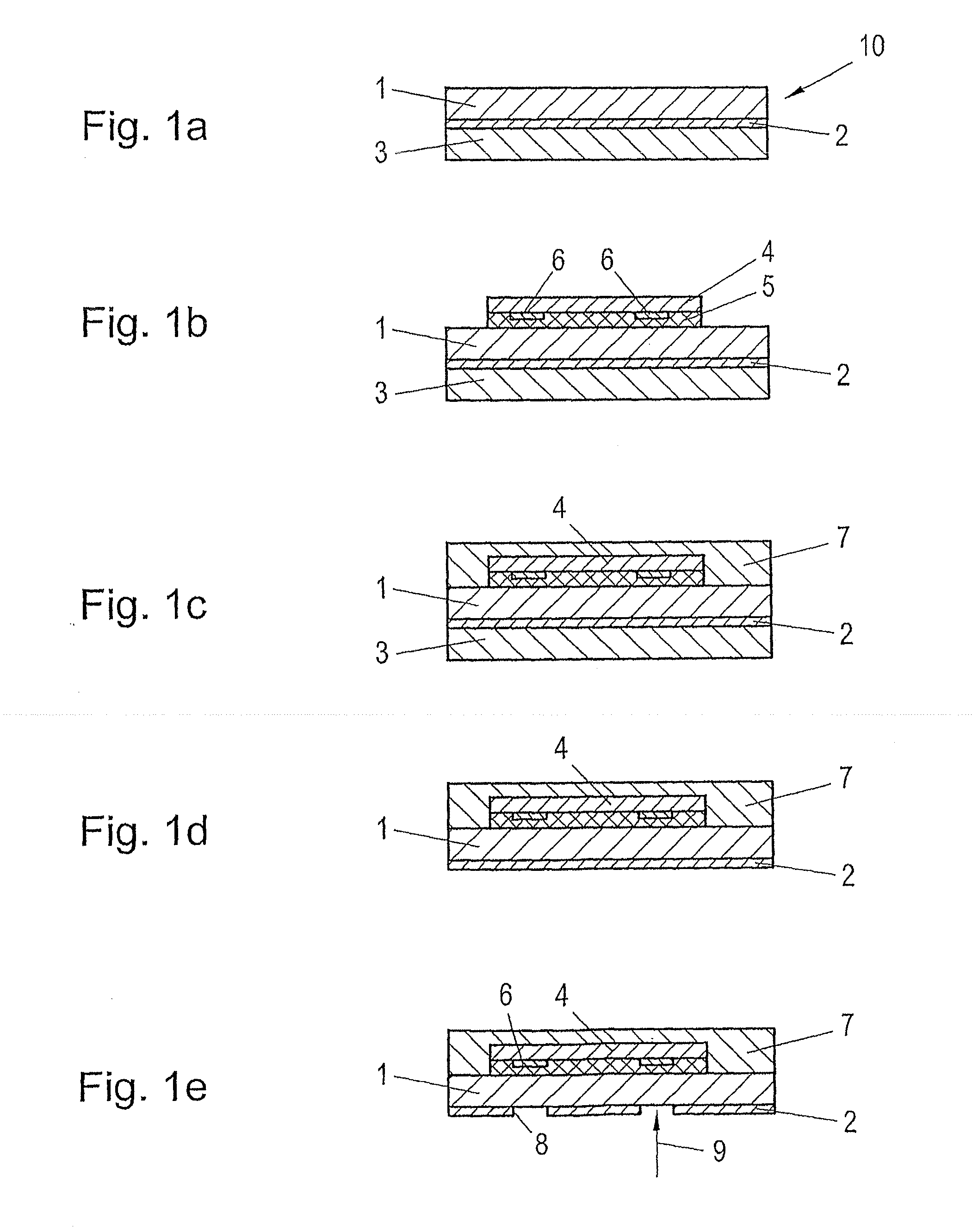
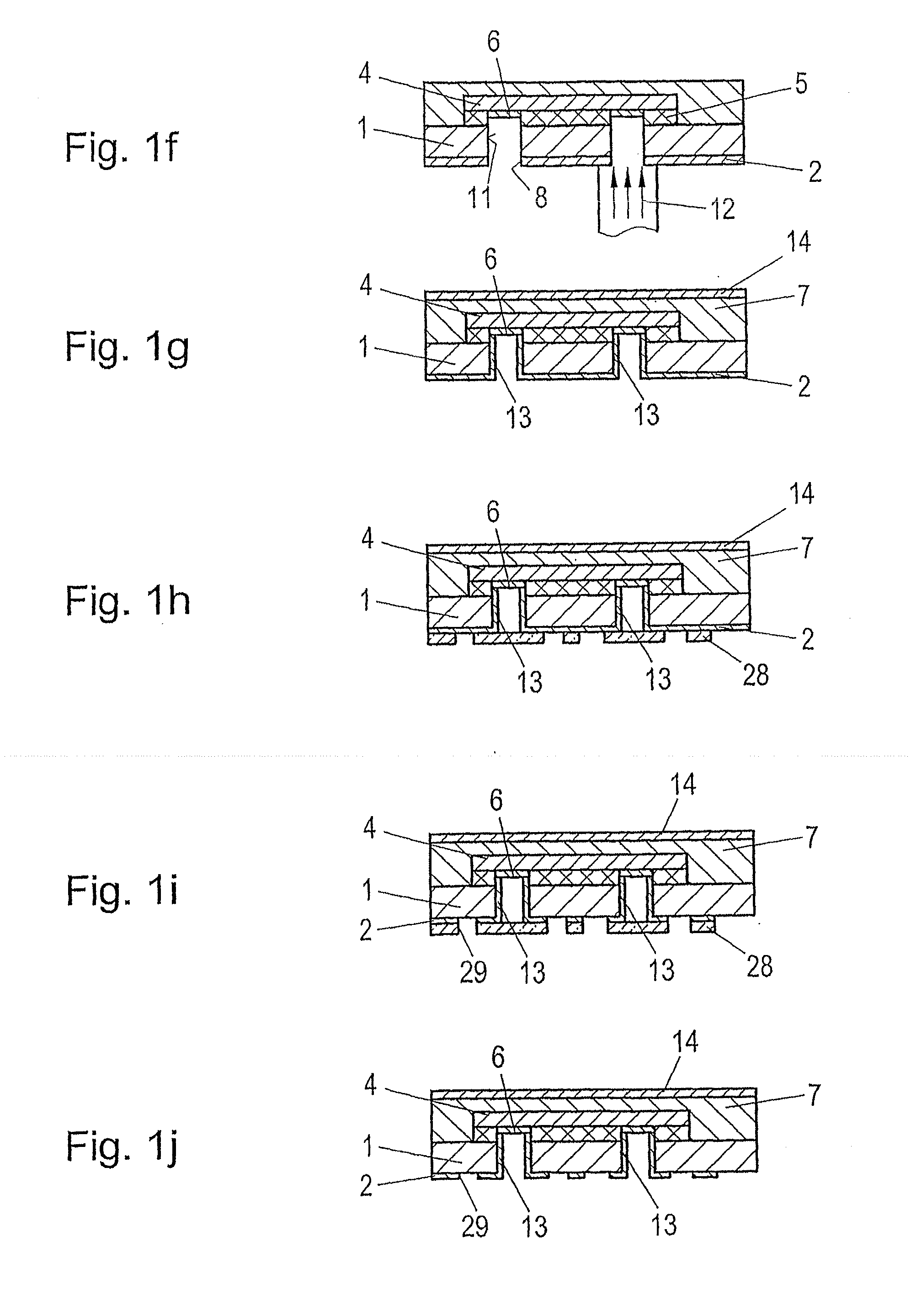
[0062]Considering the above-indicated parameters relating to the performance of the used CO2 laser, it is apparent that, due to the holes or perforations 8 made by the laser beam 9 in the method step according to FIG. 1e, a suitable cover of the insulating layer 1 located therebehind is provided for forming holes 11 that are contoured according to the contacts 6.

[0063]When providing a larger thickness for the insulating layer 1 and / or an adhesive 5 having a higher filler content, and / or for the formation of larger holes or perforations 11, a CO2 laser having an accordingly higher power according to the following Example 2 can be employed.

example 2

[0064]Thick insulating layer (30-50 μm) and / or adhesive with higher filler content

[0065]Pulsed CO2 laser

[0066]Power: 4 watts

[0067]Beam diameter: 280 μm

[0068]Pulse duration: 8 μs

[0069]Number of pulses: 13

[0070]Hole diameter: 120 μm

[0071]In this manner, even large holes or perforations 11 can be produced in an accordingly short time.

[0072]After the production or formation of the further conducting layer 13 for contacting the contacts 6 of the integrated or received component 4, it is indicated in FIG. 1h in the context of a subtractive method that a photoresist 28 is applied for further processing or patterning the conducting layer 2 and, if desired, also the additional conducting layer 13.

[0073]Corresponding to the application of the photoresist 28, a patterning is formed in the conducting layer 2 in a further method step according to FIG. 1i, e.g. by an etching procedure, by making perforations or holes 29 in the conducting layer in regions that are not covered by the photoresist 28...


PUM

PropertyMeasurementUnit
Timeaaaaaaaaaa
Timeaaaaaaaaaa
Poweraaaaaaaaaa

Abstract

The invention relates to a method for integrating an electronic component into a printed circuit board, whereby the electronic component (4) comprising contacts (6) oriented towards the insulating layer (1) is fixed to a laminate at least consisting of a conducting or conductive layer (2) and a non-conducting or insulating layer (1). According to the invention, once the component (4) has been fixed to the insulating layer (1), holes or perforations (8, 11) corresponding to the contacts (6) of the component (4) are formed in the conducting layer (2) and in the insulating layer (1), the contacts coming into contact with the conducting layer (2), enabling a reliable integration or embedding of an electronic component (4) into a printed circuit board.

Description

[0001]This is a national stage of PCT / AT2009 / 000418 filed Oct. 28, 2009 and published in German, which has a priority of Austria no. GM 619 / 2008 filed Oct. 30, 2008 and Austria no. GM 529 / 2009 filed Aug. 25, 2009, hereby incorporated by reference.FIELD OF THE INVENTION[0002]The present invention relates to a method for integrating an electronic component into a printed circuit board, whereby the electronic component comprising contacts oriented towards the insulating layer is fixed to a laminate at least consisting of a conducting or conductive layer and a non-conducting or insulating layer.PRIOR ART[0003]In the context of growing product functionalities of apparatus provided with electronic components and the increasing miniaturization of such electronic components as well as the increasing number of electronic components to be loaded on printed circuit boards, efficient field-likely or array-likely configured components or packages including several electronic components comprisin...

Claims


Application Information

Patent Timeline
IPC IPC(8): H05K3/30
CPCH01L21/6835Y10T29/49126H01L23/544H01L24/24H01L24/82H01L24/83H01L2221/68345H01L2223/54426H01L2223/54473H01L2224/2402H01L2224/83121H01L2224/83192H01L2224/8385H01L2224/92144H01L2924/01004H01L2924/01005H01L2924/01013H01L2924/01029H01L2924/01032H01L2924/01033H01L2924/01047H01L2924/01074H01L2924/01078H01L2924/01082H01L2924/078H01L2924/07802H05K1/185H05K1/188H05K3/0035H05K3/0038H05K3/025H05K3/305H05K2201/0355H05K2201/09509H05K2201/09918H05K2201/10674H05K2201/10977H05K2203/0554H05K2203/108H05K2203/1469H01L24/29H01L24/32H01L2224/32225H01L2924/01006H01L2924/014H01L23/5389Y10T29/49146H01L2924/3512H01L2924/00H01L2224/83132H01L2224/83005H01L2224/04105H05K3/46H05K1/18
Inventor SCHRITTWIESER, WOLFGANGLENHARDT, PATRICKMERL, KLAUS
Owner AT & S AUSTRIA TECH & SYSTTECHN AG
Why Eureka
Try Eureka