
Methods for improving the quality of structures comprising semiconductor materials

Active Publication Date: 2011-09-01
ARIZONA STATE UNIVERSITY +1
View PDF10 Cites 16 Cited by
  • Summary
  • Abstract
  • Description
  • Claims
  • Application Information

AI Technical Summary

Benefits of technology

[0007]Generally, methods of the present invention produce better-quality, following semiconductor layers (or “final” or “overlying” or “over grown” layers, or the like) by taking advantage of certain types of dislocations commonly found in poorer-quality starting layers (or “substrates”, “initial” or “underlying” layers, or the like).
[0008]It has been found that, up to a point, the more prominent the surface extent of dislocations in a starting or underlying surface, the better the quality of a following layer ultimately fabricated from such a starting or underlying surface. It is believed (but without intended limitation) that this surprising outcome results from the interplay of a number of factors.
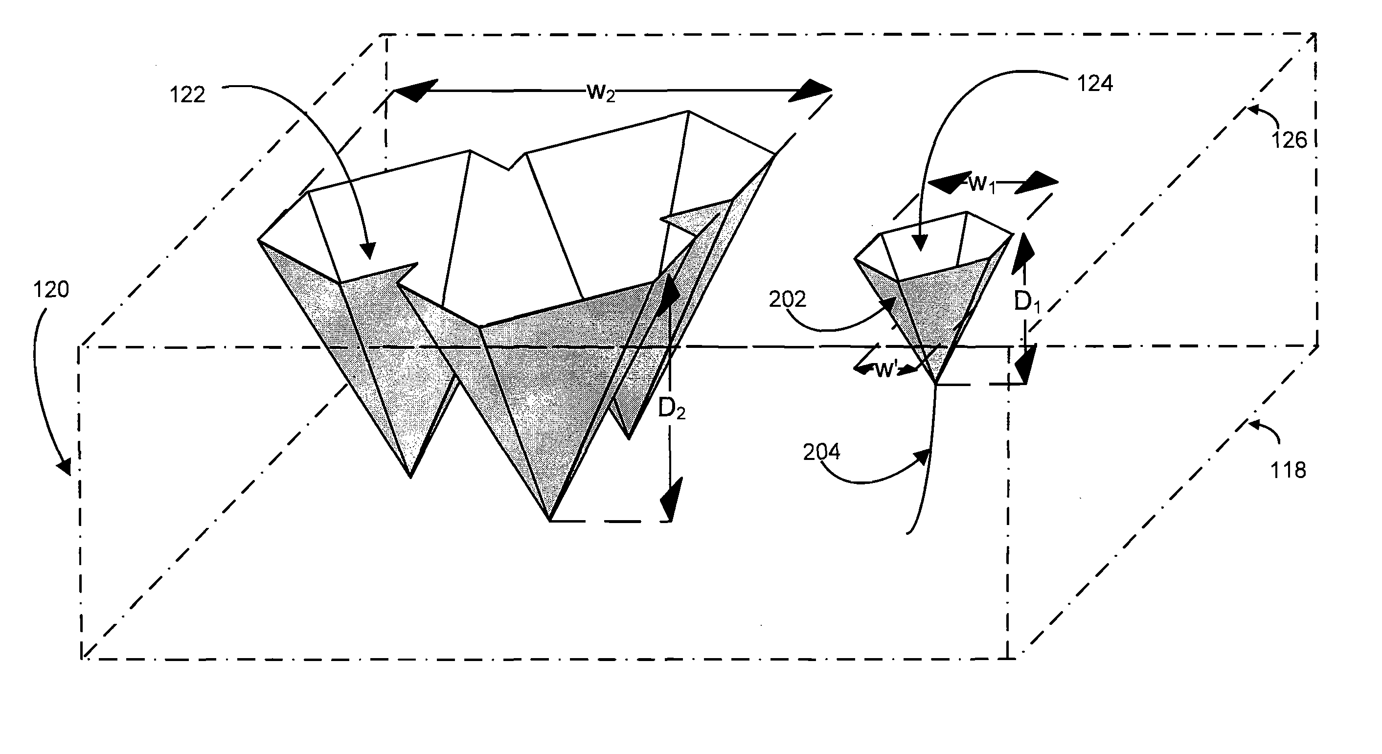
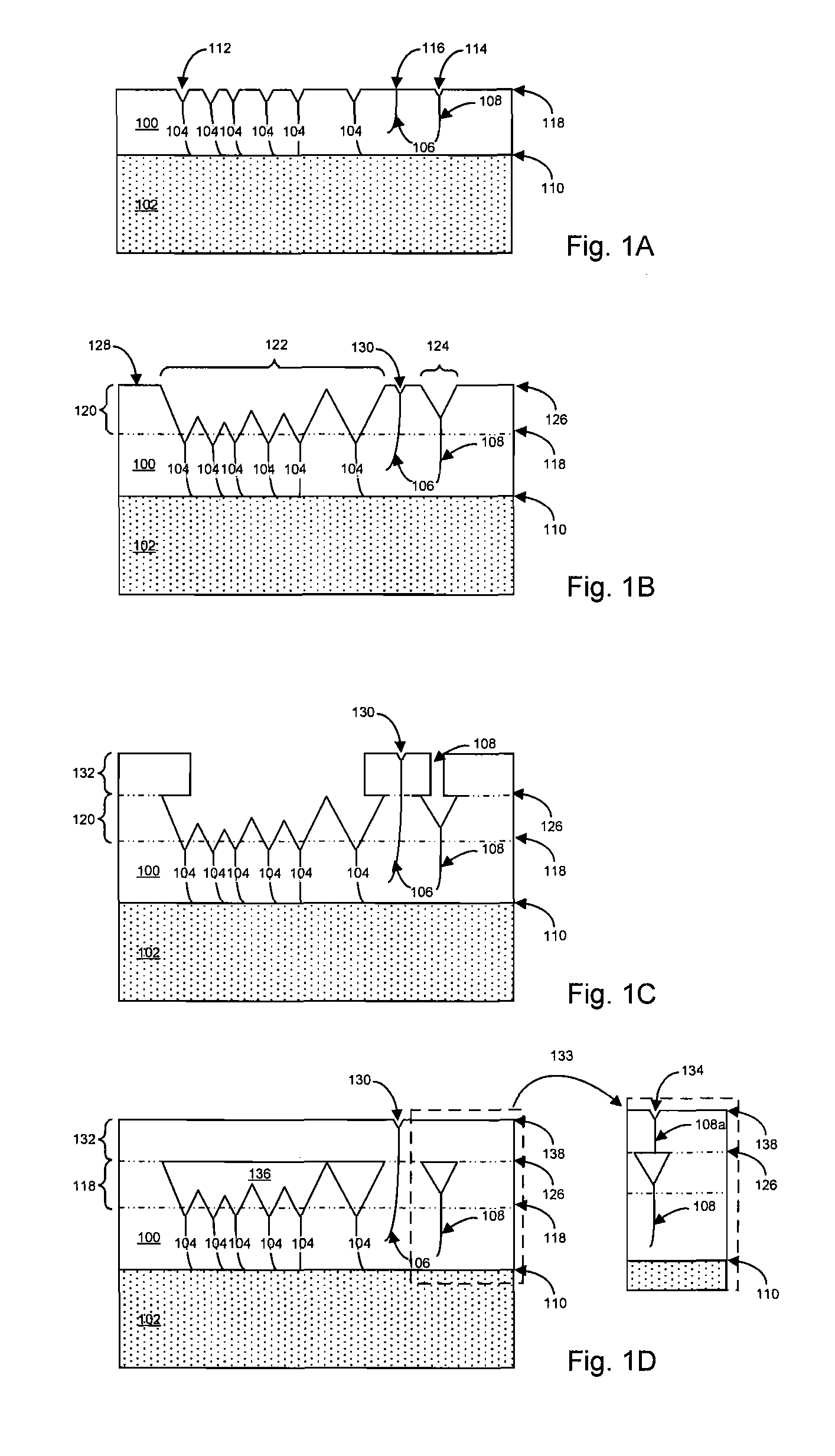
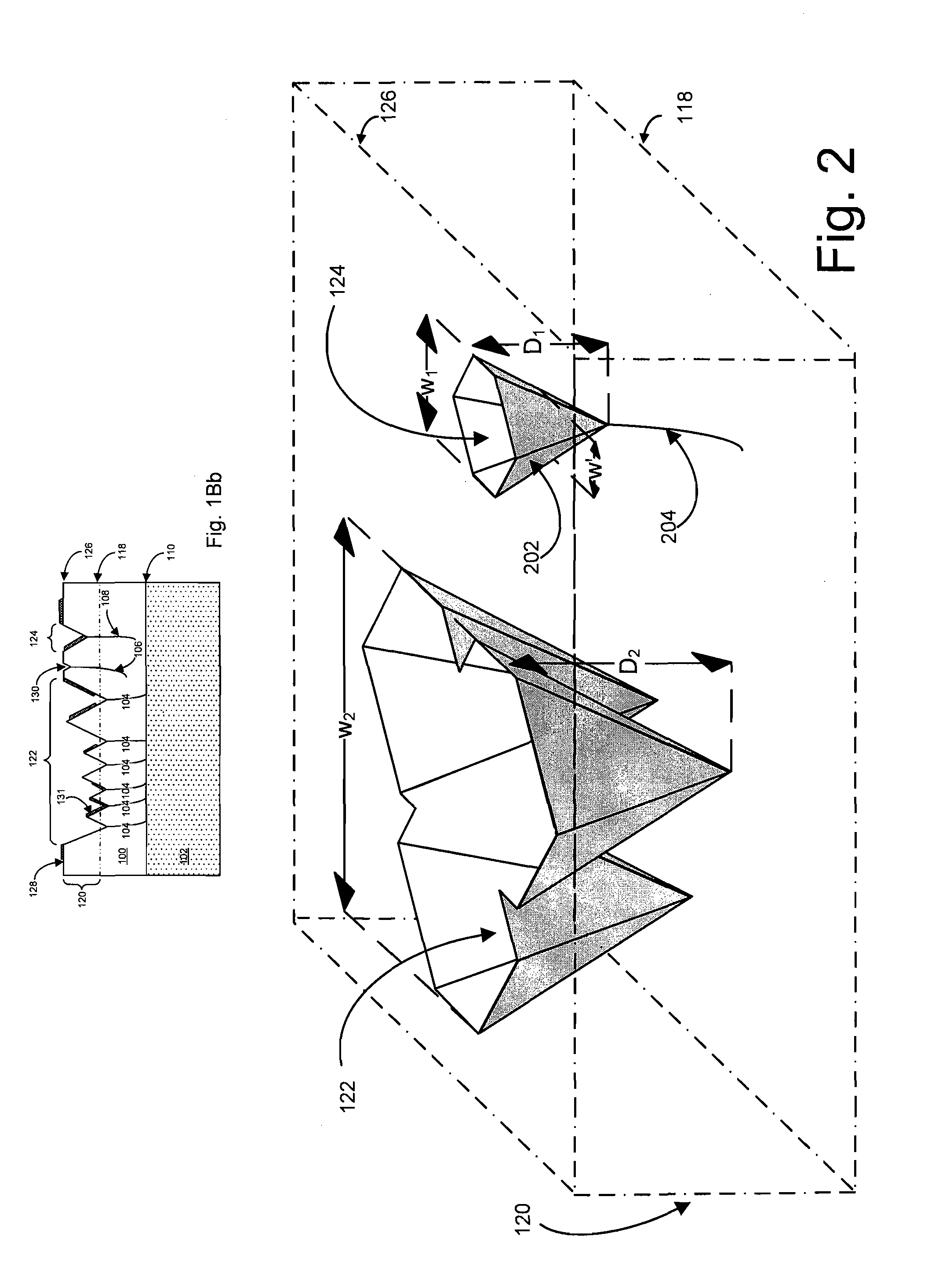
[0009]First, the dislocations in an underlying semiconductor surface may be enclosed and terminated, in such a manner, and a final layer can be grown in such a manner, that the terminated dislocations do not propagate into the final layer. The final layer can then have fewer dislocations than the underlying surface because those dislocations in the underlying surface that have been successfully enclosed and terminated are not represented in the final layer. Second, it has been found that the common surface indentation (e.g. a pit like structure) spontaneously produced at dislocations in an underlying surface can be enhanced, e.g., made larger in surface cross section (e.g. increased in size for both lateral and depth dimensions), such that they can be more effectively terminate associated dislocations when compared with less enhanced dislocations. Finally, it has been found that conditions encouraging the intersection of two or more enhanced dislocations further enhances the termination of associated dislocations and thus increases both the dislocation termination efficiency and the efficiency of dislocation reduction. Accordingly, a final layer grown from an underlying surface having enhanced and enclosed dislocations can then have even fewer dislocations than the underlying layer.
[0010]Briefly, beginning with an underlying surface of a suitable semiconductor material, methods of the invention fabricate a following layer of improved quality by steps comprising enhancing the common surface indentation spontaneously produced at selected dislocations present at the underlying surface. Subsequent processes then grow a following layer having few or no dislocations arising from the enhanced dislocations in the underlying surface.
[0017]In preferred embodiments, prior to terminating the dislocations, the invention includes depositing a discontinuous film of a dielectric material, such as a silicon nitride or oxide in the case of a III-nitride semiconductor. By choice of appropriate deposition (and / or post deposition conditions), it has been found that the dielectric material deposits discontinuously so as to reduce the number of dislocations in the laterally growing material. It is believed that this is because the discontinuous deposition occurs in the disordered regions about emergent dislocations so as to discourage subsequent lateral growth from more disordered regions about the emergent dislocations (which would promote the propagation of dislocations into the growing material) and to encourage subsequent lateral growth from less disordered regions about dislocations (which hinders the propagation of dislocations into the laterally growing material).

Problems solved by technology

Solid-state devices can suffer from inferior lifetimes and operating characteristics when the semiconductor material has an undesirable density of crystal defects, for example dislocations.
For many of these materials suitable and commercially useful growth substrates have limited availability and poor crystal quality.
A suitable substrate closely matches the crystal properties of the target material to be grown; if these properties do not closely match, the resulting material usually has an unacceptable density of dislocations.
However, these common methods often utilize lithographically produced masking elements that often produce materials with a non-uniform distribution of surface dislocations, undesirable in many applications.

Method used


Image

  • Methods for improving the quality of structures comprising semiconductor materials
  • Methods for improving the quality of structures comprising semiconductor materials
  • Methods for improving the quality of structures comprising semiconductor materials

Examples


examples

[0130]The following examples and reports of experiments illustrate etch pitting, enlargement of pits, amorphous Si3N4 deposition and epitaxial lateral overgrowth (ELOG) that were carried out on a two-step GaN substrate to develop the optimum protocols for the reduction of threading dislocations.

[0131]In the GaN etch pit studies, ex-situ aqueous KOH etching, molten KOH etching, and in-situ SiH4 etching were carried out at temperatures of 80° C., 260° C., and 860° C. with different etching periods in the range of 0 to 10 mins, respectively. Ex-situ aqueous KOH etching (Han et al. Scripta Materialia 59 1171 2008) and an in-situ SiH4 etching method were used to delineate etch pits associated with dislocations and to determine threading dislocation density. In general, a transmission electron microscope (TEM)-based technique could be used to reveal all types of threading dislocations (TDs) and to measure the TD density in GaN with high contrast over a relatively large area. As this requi...


PUM


Abstract

Methods which can be applied during the epitaxial growth of semiconductor structures and layers of III-nitride materials so that the qualities of successive layers are successively improved. An intermediate epitaxial layer is grown on an initial surface so that growth pits form at surface dislocations present in the initial surface. A following layer is then grown on the intermediate layer according to the known phenomena of epitaxial lateral overgrowth so it extends laterally and encloses at least the agglomerations of intersecting growth pits. Preferably, prior to growing the following layer, a discontinuous film of a dielectric material is deposited so that the dielectric material deposits discontinuously so as to reduce the number of dislocations in the laterally growing material. The methods of the invention can be performed multiple times to the same structure. Also, semiconductor structures fabricated by these methods.

Description

CROSS-REFERENCE TO RELATED APPLICATIONS[0001]This application is a continuation-in-part of application Ser. No. 12 / 618,500 filed Nov. 13, 2009 and claims the benefit of application No. 61 / 114,855 filed Nov. 14, 2008. The entire disclosure of each prior application is expressly incorporated herein by reference thereto.FIELD OF THE INVENTION[0002]The invention relates to the fabrication of semiconductor structures, and in particular to the epitaxial growth of high crystal quality structures comprising III-nitride materials. Embodiments of the invention include methods for improving the crystal quality of a semiconductor structure, and structures fabricated utilizing these methods.BACKGROUND OF THE INVENTION[0003]The quality of a semiconductor material can considerably influence the performance of a solid-state device produced from said material. Solid-state devices can suffer from inferior lifetimes and operating characteristics when the semiconductor material has an undesirable densi...

Claims


Application Information

Patent Timeline
IPC IPC(8): H01L21/20
CPCH01L21/02458H01L21/0254H01L21/02647H01L21/02639H01L21/0262
Inventor ARENA, CHANTALHAN, ILSU
Owner ARIZONA STATE UNIVERSITY
Learn More