Electrode and plasma processing apparatus

a plasma processing and electrode technology, applied in the direction of electric discharge tubes, coatings, chemical vapor deposition coatings, etc., can solve the problem that it is more difficult for a high frequency power to escape from the fine holes of the base than from other areas

Active Publication Date: 2011-09-22
TOKYO ELECTRON LTD
View PDF5 Cites 12 Cited by
  • Summary
  • Abstract
  • Description
  • Claims
  • Application Information

AI Technical Summary

Benefits of technology

[0013]Based on this principle, in the present disclosure, by forming the multiple number of fine holes at the central area of the base serving as the electrode, an electrostatic capacitance at the central area of the base is reduced to be lower than an electrostatic capacitance at a periphery thereof. Accordingly, it is possible to achieve an effect equal to a case in which the dielectric member serving as the base becomes thicker at the central area than the periphery thereof. That is, it is more difficult for a high frequency power to escape from the fine holes of the base than to escape from other areas. Consequently, in the present disclosure, by using the electrode made of only a homogeneous material (i.e. the base having the dielectric constant ∈), plasma density at the central area of the base can be reduced, so that an intensity distribution of an electric field of a high frequency power used for generating plasma can be uniform (hereinafter, referred to as uniformization effect due to an upper electrode).
[0014]Conventionally, by embedding the different member having a lower dielectric constant than that of the conductor in the central area of the conductor, plasma density at the central area of the conductor was reduced and a distribution of the plasma density became uniform. However, as described above, there is no material having a lower dielectric constant than that of a vacuum. For this reason, if a fine hole having a vacuum state therein is used in accordance with the present disclosure, a difference in a dielectric constant between the base and the file hole can be increased as compared to a case in which any other dielectric member is inserted into the base, and it is possible to achieve the uniformization effect due to an upper electrode.
[0015]Further, in the present disclosure, there is no need to connect the conductor with the dielectric member, and, thus, a certain material or a certain adhesive is not needed. Besides, with respect to a plate-shaped member, the fine holes are formed at an area thereof where the uniformization effect due to an upper electrode is required, and, thus, it becomes easy and simple to manufacture the plate-shaped member and there is no need to redesign a whole ceiling plate. Since the fine holes having a hollow region therein are just formed in the base, the adhesive does not peeled off and comes out to the processing chamber. For this reason, the present disclosure has an excellent effect due to the upper electrode, which is effective particularly with respect to a ceiling plate which is made of only a high purity material because of strict demands for a process against metal contamination.
[0016]The diameter of the fine hole is equal to or less than twice the thickness of the sheath. For this reason, an inner space of the fine hole may become a sheath region. Consequently, it is possible to avoid a generation of abnormal electric discharge within the fine hole and possible to prevent plasma from being introduced into the fine hole.
[0028]As described above, in accordance with the present disclosure, it is possible to control an intensity distribution of a high frequency electric field used for generating plasma by using an electrode made of a homogeneous material.

Problems solved by technology

That is, it is more difficult for a high frequency power to escape from the fine holes of the base than to escape from other areas.

Method used


Image

  • Electrode and plasma processing apparatus
  • Electrode and plasma processing apparatus
  • Electrode and plasma processing apparatus

Examples


Embodiment Construction

[0035]Hereinafter, embodiments of the present disclosure will be described in detail with reference to the accompanying drawings. Through the present specification and drawings, parts having substantially same function and configuration will be assigned same reference numerals, and redundant description will be omitted.

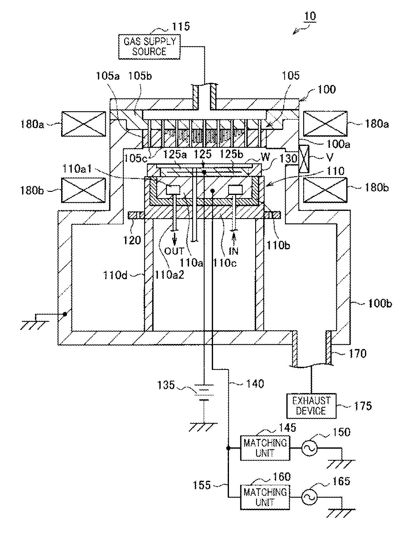
[0036]An RIE plasma etching apparatus (parallel plate type plasma processing apparatus) using an electrode in accordance with an embodiment of the present disclosure will be explained with reference to FIG. 1. An RIE plasma etching apparatus 10 is an example of a plasma processing apparatus that introduces a processing gas into a depressurizable processing chamber, generates plasma by a high frequency power and performs a plasma process on a processing target object by the plasma.

[0037]The RIE plasma etching apparatus 10 may include a depressurizable processing chamber 100. The processing chamber 100 may include an upper chamber 100a of a small diameter and a lower ch...


PUM

PropertyMeasurementUnit
frequencyaaaaaaaaaa
frequencyaaaaaaaaaa
diameteraaaaaaaaaa

Abstract

There is provided a plasma processing apparatus including a processing chamber 100 configured to perform a plasma process on a wafer W; an upper electrode 105 and a lower electrode 110 arranged to face each other in the processing chamber 100 and configured to form a processing space therebetween; and a high frequency power supply 150 connected with at least one of the upper electrode 105 and the lower electrode 110 and configured to output a high frequency power into the processing chamber 100. The upper electrode 105 includes an upper base 105a made of a dielectric material, and a plurality of fine holes A having a diameter equal to or less than twice a thickness of a sheath are formed in the upper base 105a.

Description

CROSS-REFERENCE TO RELATED APPLICATION[0001]This application claims the benefit of Japanese Patent Application No. 2010-059485 filed on Mar. 16, 2010 and U.S. Provisional Application Ser. No. 61 / 323,051 filed on Apr. 12, 2010, the entire disclosures of which are incorporated herein by reference.FIELD OF THE INVENTION[0002]The present disclosure relates to a structure of an electrode used in a plasma processing apparatus and a plasma processing apparatus using this electrode. To be more specific, the present disclosure relates to a structure of an electrode used in a plasma processing apparatus for controlling an intensity distribution of a high frequency electric field used for generating plasma and a plasma processing apparatus using this electrode.BACKGROUND OF THE INVENTION[0003]Recently, as miniaturization is increasingly demanded, a relatively high frequency power needs to be supplied to generate high density plasma. As depicted in FIG. 6, as a frequency of a power supplied fro...

Claims


Application Information

Patent Timeline
Patent Type & Authority Applications(United States)
IPC IPC(8): C23F1/08C23C16/455C23C16/50
CPCH01J37/32091H01J37/3266H01J37/32541
Inventor HAYASHI, DAISUKEMATSUYAMA, SHOICHIROMURAKAMI, KOICHI
Owner TOKYO ELECTRON LTD
Why Eureka
Try Eureka