Semiconductor device and driving method of semiconductor device

a technology of semiconductor devices and semiconductor devices, applied in the direction of solid-state devices, capacitors, instruments, etc., can solve the problems of long time-consuming storage of semiconductor devices, and achieve the effects of increasing the degree of integration of semiconductor devices, reducing the area occupied by memory cells, and increasing storage capacity per unit area

Inactive Publication Date: 2011-09-22
SEMICON ENERGY LAB CO LTD
View PDF99 Cites 37 Cited by
  • Summary
  • Abstract
  • Description
  • Claims
  • Application Information

AI Technical Summary

Benefits of technology

[0027]In a semiconductor device according to the disclosed invention, transistors each including an oxide semiconductor in memory cells of the semiconductor device are connected in series; thus, a source electrode of the transistor including an oxide semiconductor in the memory cell and a drain electrode of the transistor including an oxide semiconductor in the adjacent memory cell can be connected to e

Problems solved by technology

When a semiconductor material which allows a sufficient reduction in off-state curr

Method used


Image

  • Semiconductor device and driving method of semiconductor device
  • Semiconductor device and driving method of semiconductor device
  • Semiconductor device and driving method of semiconductor device

Examples


embodiment 1

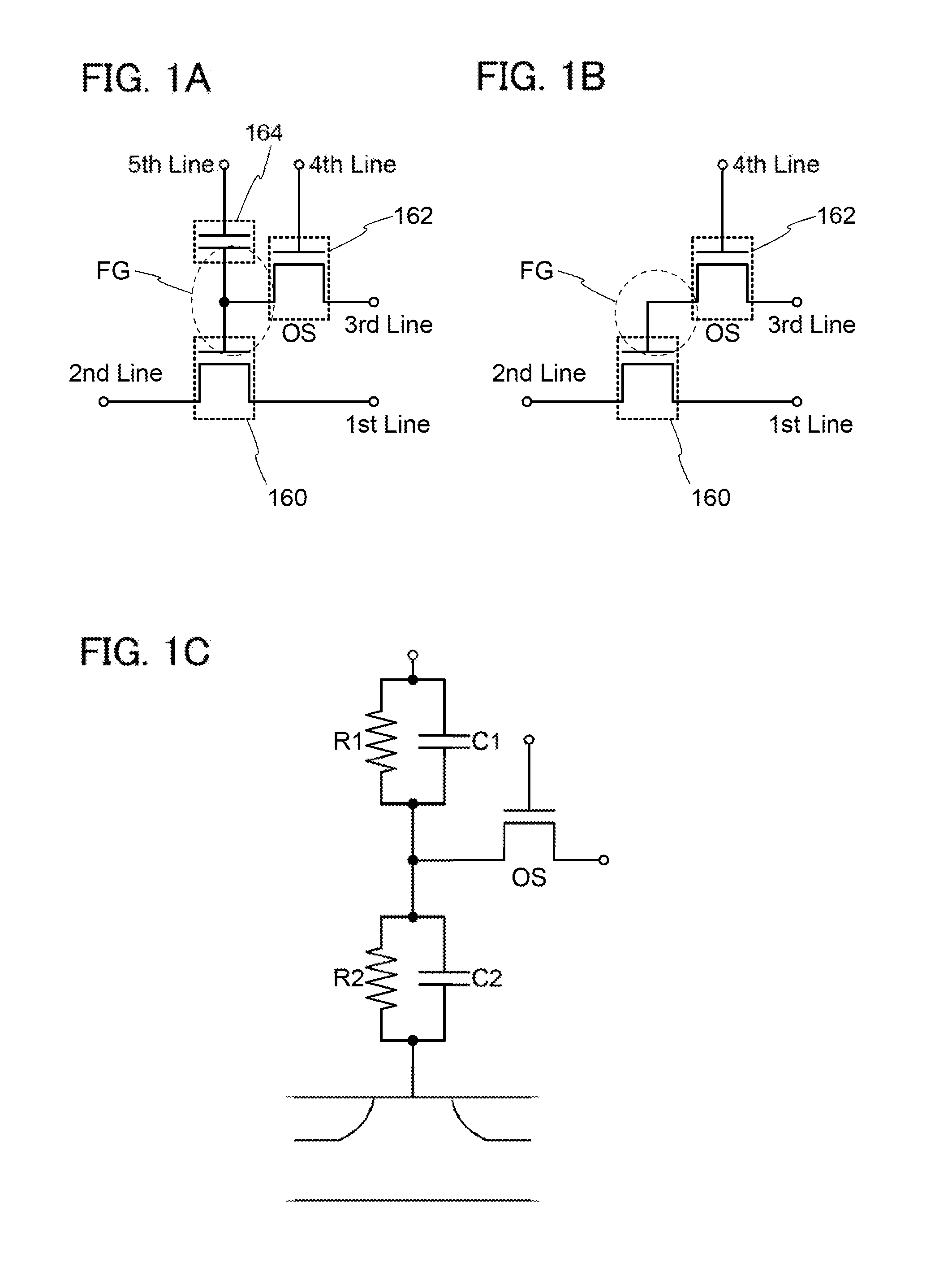
[0044]In this embodiment, a circuit structure and operation of a semiconductor device according to one embodiment of the disclosed invention, will be described with reference to FIGS. 1A to 1C, FIG. 2, FIG. 3, FIG. 4, and FIG. 5. Note that in each of the circuit diagrams, “OS” may be written, beside a transistor in order to indicate that the transistor includes an oxide semiconductor.

[0045]First, the basic circuit structure and its operation will be described with reference to FIGS. 1A to 1C. In the semiconductor device in FIG. 1A, a first wiring (a 1st line) and a source electrode (or a drain electrode) of a transistor 160 are electrically connected to each other, and a second wiring (a 2nd line) and the drain electrode (or the source electrode) of the transistor 160 are electrically connected to each other. In addition, a third wiring (a 3rd line) and a source electrode (or a drain electrode) of a transistor 162 are electrically connected to each other, and a fourth wiring (a 4th ...

application example

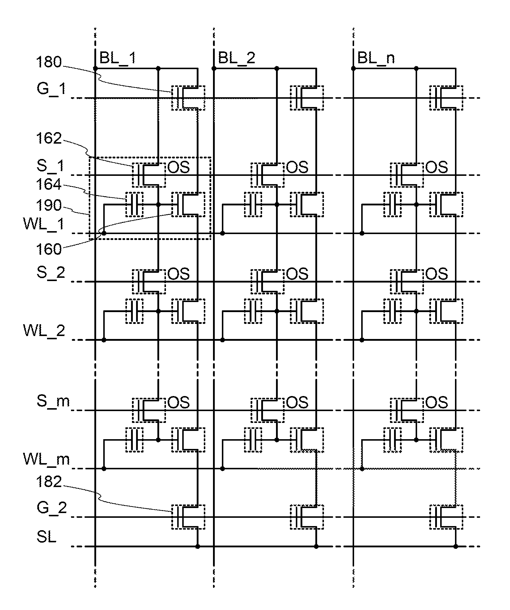
[0071]Next, a more specific circuit structure to which the circuit illustrated in FIGS. 1A to 1C is applied and an operation thereof will be described with reference to FIG. 2, FIG. 3, FIG. 4, and FIG. 5.

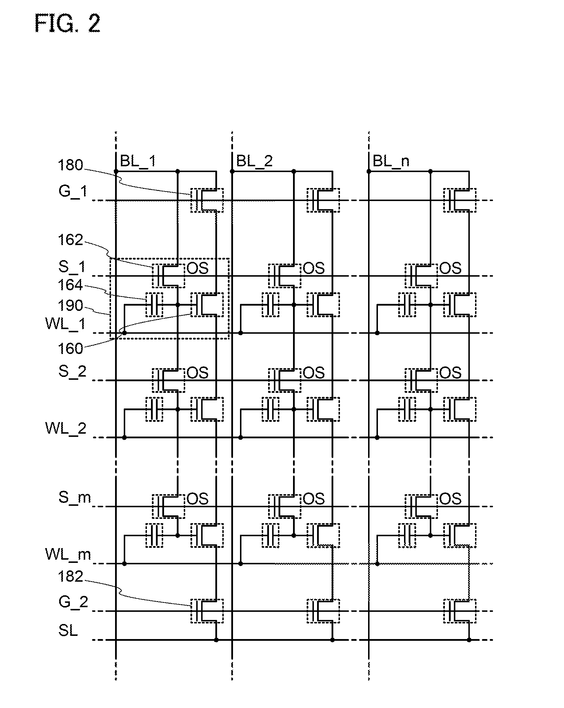
[0072]FIG. 2 is an example of a circuit diagram of a semiconductor device including m (rows) (in a vertical direction)×n (columns) (in a horizontal direction) memory cells 190. The structure of the memory cells 190 in FIG. 2 is similar to that in FIG. 1A, That is, the first wiring and the third wiring in FIG. 1A correspond to a hit line BL in FIG. 2; the second wiring in FIG. 1A, a source line SL in FIG. 2; the fourth wiring in FIG. 1A, a signal line S in FIG. 2; and the fifth wiring in FIG. 1A, a word line WL in FIG. 2. Note that in FIG. 2, the memory cells 190 in a column direction are connected in series in such a manner that the transistors 162 are connected in series and the transistors 160 are connected in series; thus, only the memory cells 190 in the first row are connected ...

embodiment 2

[0108]In this embodiment, a structure and a manufacturing method of a semiconductor device according to one embodiment of the disclosed invention will be described with reference to FIGS. 6A and 6B, FIGS. 7A and 7B, FIGS. 8A to 8C, FIGS. 9A to 9D, FIGS. 10 to 10D, FIGS. 11A to 11D, and FIGS. 12A to 12D.

[0109]FIGS. 6A and 6B illustrate an example of a structure of the memory cell 190 and the selection transistor 180 in the semiconductor device illustrated in the circuit diagram of FIG. 2. FIG. 6A illustrates a cross section of the semiconductor device, and FIG. 6B illustrates a plan view of the semiconductor device. Here, FIG. 6A illustrates a cross section taken along line A1-A2 in FIG. 6B. In FIG. 6B, a direction parallel to line A1-A2 corresponds to the column direction in the circuit diagram of FIG. 2, and a direction perpendicular to line A1-A2 corresponds to the row direction in the circuit diagram of FIG. 2. The semiconductor device illustrated in FIGS. 6A and 6B includes the ...


PUM


Abstract

A semiconductor device is formed using a material which allows a sufficient reduction in off-state current of a transistor; for example, an oxide semiconductor material, which is a wide-gap semiconductor, is used. When a semiconductor material which allows a sufficient reduction in off-state current of a transistor is used, the semiconductor device can hold data for a ions time. Transistors each including an oxide semiconductor in memory cells of the semiconductor device are connected in series; thus, a source electrode of the transistor including an oxide semiconductor in the memory cell and a drain electrode of the transistor including an oxide semiconductor in the adjacent memory cell can be connected to each other. Therefore, the area occupied by the memory cells can be reduced.

Description

TECHNICAL FIELD[0001]The disclosed invention relates to a semiconductor device including a semiconductor element and a driving method of the semiconductor device.BACKGROUND ART[0002]Memory devices using semiconductor elements are broadly classified into two categories: a volatile device that loses stored data when not powered, and a non-volatile device that holds stored data even when not powered.[0003]A typical example of a volatile memory device is a dynamic random access memory (DRAM). A DRAM stores data in such a manner that a transistor included in a memory element is selected and charge is accumulated in a capacitor.[0004]Owing to the above principle, charge in the capacitor is lost when data in a DRAM is read out; thus, another writing operation is necessary every time data is read out. Moreover, since leakage current (off-state current) flows between a source and a drain of a transistor included in a memory element when the transistor is in an off state, charge flows into or...

Claims


Application Information

Patent Timeline
IPC IPC(8): H01L27/108
CPCG11C16/0408H01L27/115H01L27/11521H01L28/60H01L27/1207H01L27/1225H01L27/13H01L27/1156H10B41/70H10B69/00H10B41/30H01L27/0688H10B12/00
Inventor KATO, KIYOSHIOKAMOTO, SATOHIRONAGATSUKA, SHUHEI
Owner SEMICON ENERGY LAB CO LTD
Why Eureka
Try Eureka