Schottky barrier semiconductor device

a technology of semiconductor devices and shields, applied in semiconductor devices, basic electric elements, electrical equipment, etc., can solve the problems of reducing the power efficiency in high frequency regions, difficult to simultaneously minimize both these properties, and jbs commonly undergoes a great forward voltage drop, so as to increase the schottky junction area, increase the amount of forward current, and increase the chip size of the semiconductor element.

Inactive Publication Date: 2011-09-22
PANASONIC CORP
View PDF6 Cites 12 Cited by
  • Summary
  • Abstract
  • Description
  • Claims
  • Application Information

AI Technical Summary

Benefits of technology

[0066]The conventional TMBS has a large impurity concentration gradient between the semiconductor substrate and the semiconductor drift layer. Thus, electric fields concentrate between the semiconductor substrate and the semiconductor drift layer. Consequently, a low backward applied voltage makes it possible to reach the critical field intensity, causing avalanche breakdown. This prevents the backward stopping voltage from being increased.
[0077]As described above, the Schottky barrier semiconductor device in accordance with the preset invention is efficient because of the reduced backward leakage current, the increased stopping voltage, the reduced forward voltage drop, and the improved power efficiency compared to the conventional TMBS. The Schottky barrier semiconductor device in accordance with the present invention also has a high durability against the surge and transient voltage.

Problems solved by technology

This makes it difficult to simultaneously minimize both of these properties.
However, the JBS commonly undergoes a great forward voltage drop.
This reduces the power efficiency in high frequency regions.
This results in a breakdown voltage higher than that of the ideal parallel-plane PN junction semiconductor device.
Further, the absence of PN junctions prevents the possible transmission of minority carriers even when a large current flows forward.
This in turn prevents a decrease in power efficiency in high frequency regions.
However, increasing the impurity concentration makes it difficult to deplete the mesa portion during the application of the backward voltage.
This increases the backward leakage current.
This in turn results in the tradeoff relationship between the breakdown voltage and the backward leakage current.
Thus, even the above TMBS does not allow the provision of an efficient semiconductor device having a reduced backward leakage current, an increased stopping voltage, a reduced forward voltage drop, and an improved power efficiency.
As a result, the semiconductor device has a very low durability against the surge and transient voltage.

Method used


Image

  • Schottky barrier semiconductor device
  • Schottky barrier semiconductor device
  • Schottky barrier semiconductor device

Examples


embodiment 1

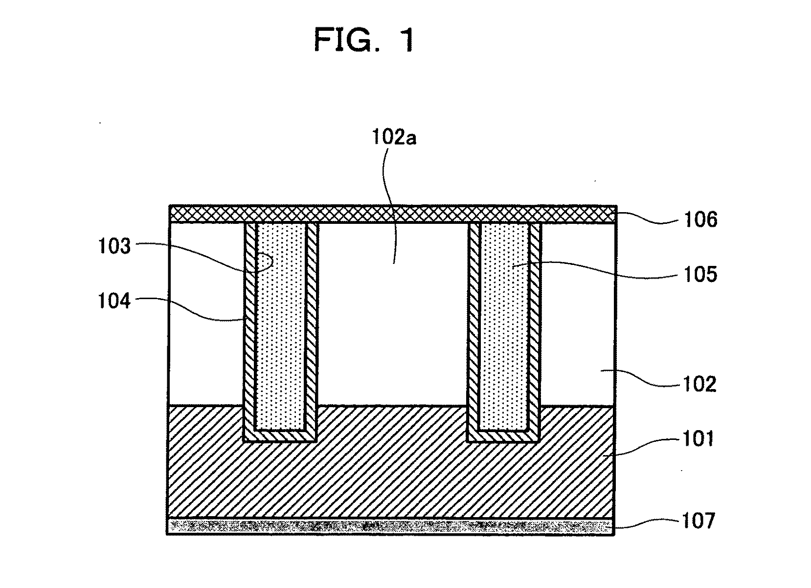
[0102]FIG. 1 shows a sectional view of a Schottky barrier semiconductor device in accordance with the present invention. In FIG. 1, the Schottky barrier semiconductor device has a semiconductor layer 102 with a low impurity concentration formed on one of the major surfaces, that is, the front and back surfaces, of a semiconductor substrate 101 of N or P conductivity type. A plurality of trenches 103 are formed in the low-concentration semiconductor layer 102. Each of the trenches 103 is shaped so as to extend from the front surface of the low-concentration semiconductor layer 102 to the semiconductor substrate 101.

[0103]A part of the semiconductor layer 102 between the trenches 103 forms a mesa portion 102a. An insulating film 104 is formed at the boundary between the mesa portion 102a and the trench 103. A first electrode 105 is formed inside the trench 103 surrounded by the insulating film 104.

[0104]A second electrode 106 is formed on the front surface of the low-concentration sem...

embodiment 2

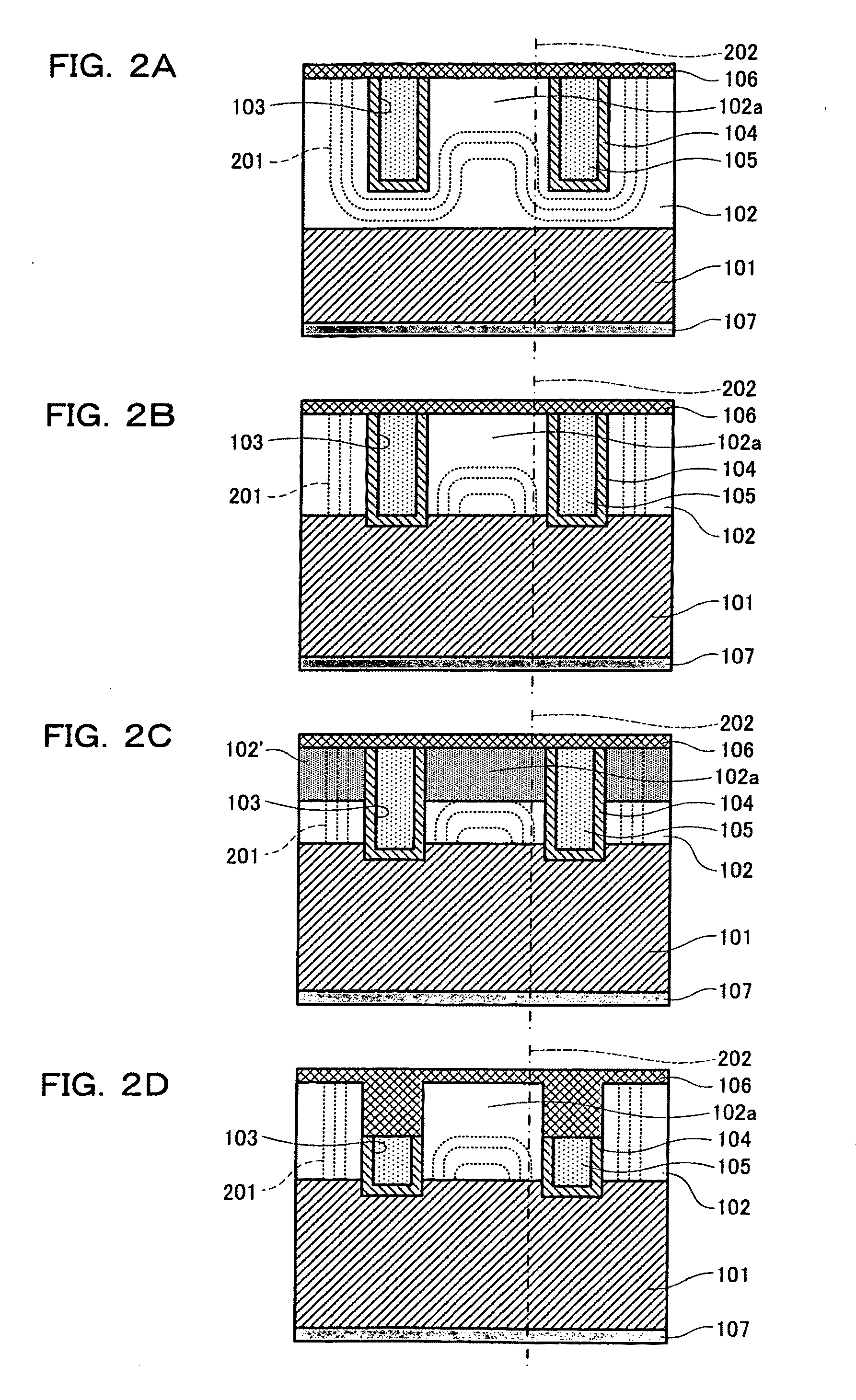
[0112]FIG. 6 is a sectional view showing another embodiment of the present invention. A lower semiconductor layer 102 having a lower impurity concentration than the semiconductor substrate 101 is formed on one of the major surfaces, that is, the front and back surfaces, of the semiconductor substrate 101. An upper semiconductor layer 102′ having a much lower impurity concentration is formed on the front surface of the lower semiconductor layer 102. At least one trench 103 is formed which extends from the front surface of the upper semiconductor layer 102′ to the semiconductor substrate 101. The mesa portion 102a is formed between the trenches 103 in both the lower and upper semiconductor layers 102 and 102′.

[0113]The insulating film 104 is formed at the boundary between the mesa portion 102a and each of the trenches 103. The first electrode 105 is formed inside the trench 103 surrounded by the insulating film 104. The second electrode 106 formed on the front surface of the low-conce...

embodiment 3

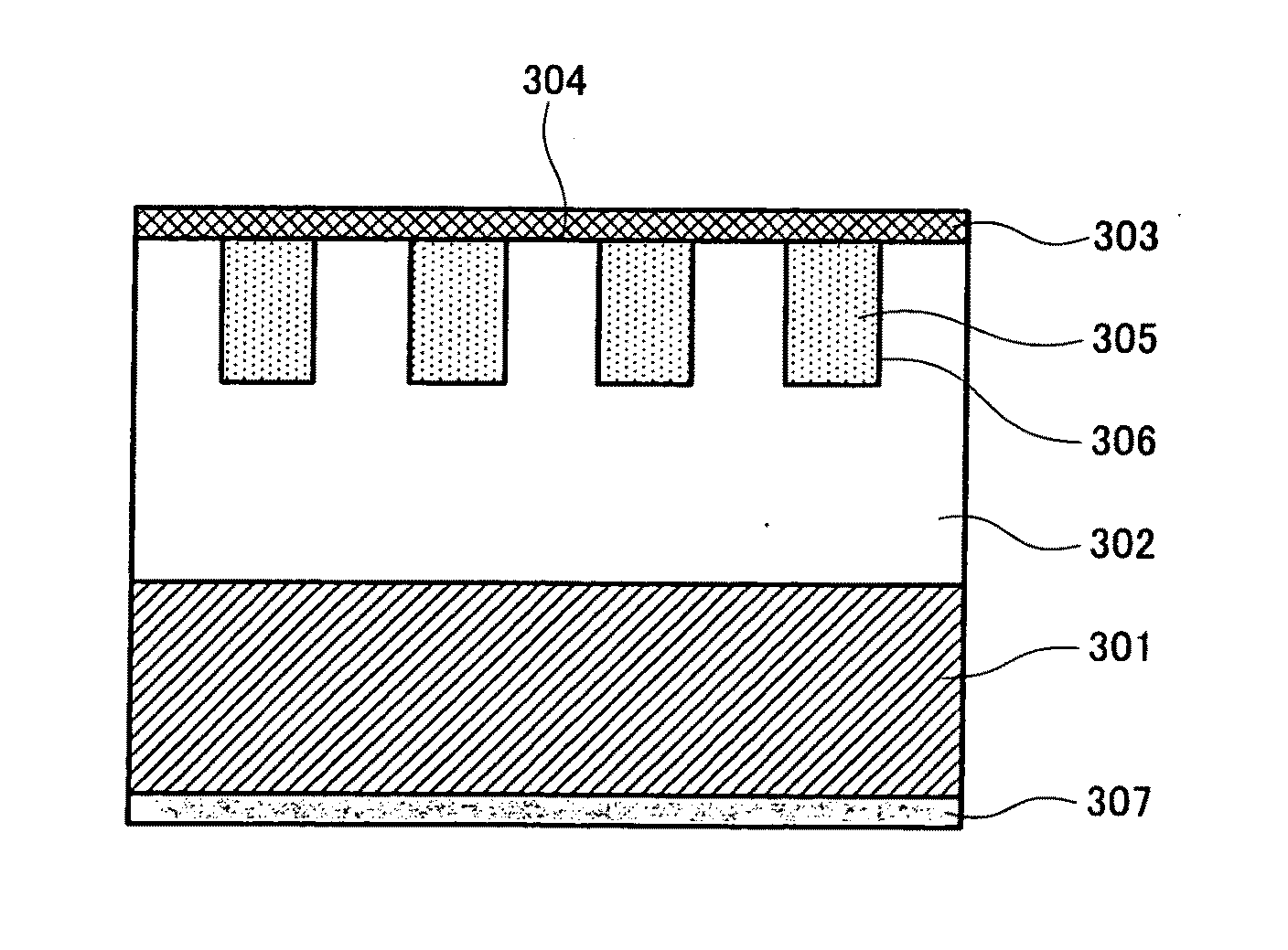
[0119]FIG. 7 shows a sectional view of another embodiment of the present invention. In FIG. 7, the Schottky barrier semiconductor device has the semiconductor layer 102 with the low impurity concentration formed on one of the major surfaces, that is, the front and back surfaces, of the semiconductor substrate 101. The plurality of trenches 103 are formed in the low-concentration semiconductor layer 102. Each of the trenches 103 is shaped so as to extend from the front surface of the low-concentration semiconductor layer 102 to the semiconductor substrate 101.

[0120]The part of the semiconductor layer 102 between the trenches 103 forms the mesa portion 102a. The insulating film 104 is formed at the boundary between the mesa portion 102a and the trench 103. The first electrode 105 is formed inside the trench 103 surrounded by the insulating film 104.

[0121]The second electrode 106 formed on the front surface of the low-concentration semiconductor layer 102 so as to cover the first elect...


PUM


Abstract

The present invention provides a Schottky barrier semiconductor device having a semiconductor substrate 101, a low-concentration semiconductor layer 102, trenches 103 formed in the low-concentration semiconductor layer 102 and extending to the semiconductor substrate 101, and a mesa portion 102a formed between the trenches 103. This provides a high durability against a surge or transient voltage.

Description

FIELD OF THE INVENTION[0001]The present invention relates to a Schottky barrier semiconductor device, and specifically, to a technique for a semiconductor device having a Schottky junction.BACKGROUND OF THE INVENTION[0002]A Schottky barrier semiconductor device exerts a rectifying effect and is applicable to a wide range of fields as shown in FIG. 23. In general, a rectifier must offer a low resistance to a forward current, while offering a very high resistance to a backward current. The rectifying effect of the Schottky barrier semiconductor device is based on transportation of a nonlinear, unipolar charge carrier (current) crossing an interface in a metal / semiconductor junction. This makes it possible to provide a large forward current with a reduced loss. Thus, the Schottky barrier semiconductor device is widely used as an output rectifier particularly for mode switching power sources such as motor driving mechanisms and high-speed power switching apparatuses.[0003]The transporta...

Claims


Application Information

Patent Timeline
Patent Type & Authority Applications(United States)
IPC IPC(8): H01L29/872
CPCH01L29/407H01L29/417H01L29/8725H01L29/872H01L29/66143
Inventor OONISHI, KAZUHIRO
Owner PANASONIC CORP
Why Eureka
Try Eureka