Solid-state image taking device and electronic apparatus
a technology of solid-state image and electronic equipment, which is applied in the direction of transistors, television systems, television system scanning details, etc., can solve the problems of ktc noise and image quality degradation, and achieve the effect of eliminating noise components and eliminating noise components
- Summary
- Abstract
- Description
- Claims
- Application Information
AI Technical Summary
Benefits of technology
Problems solved by technology
Method used
Image

Examples
first embodiment
1: First Embodiment
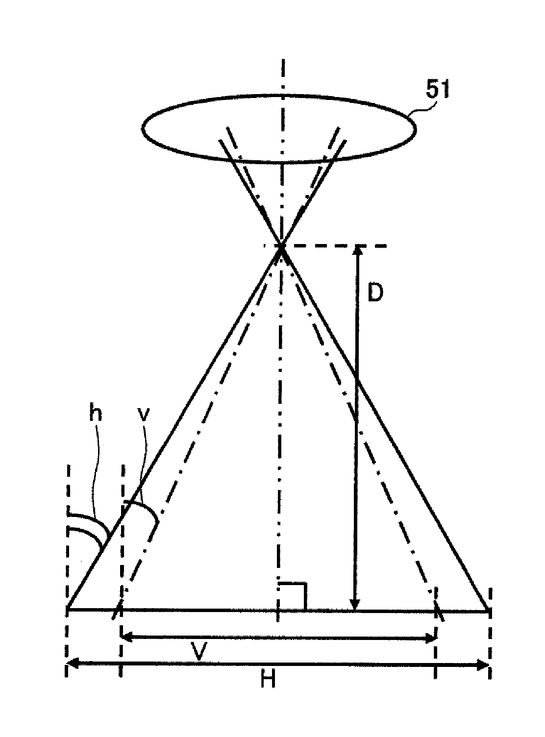
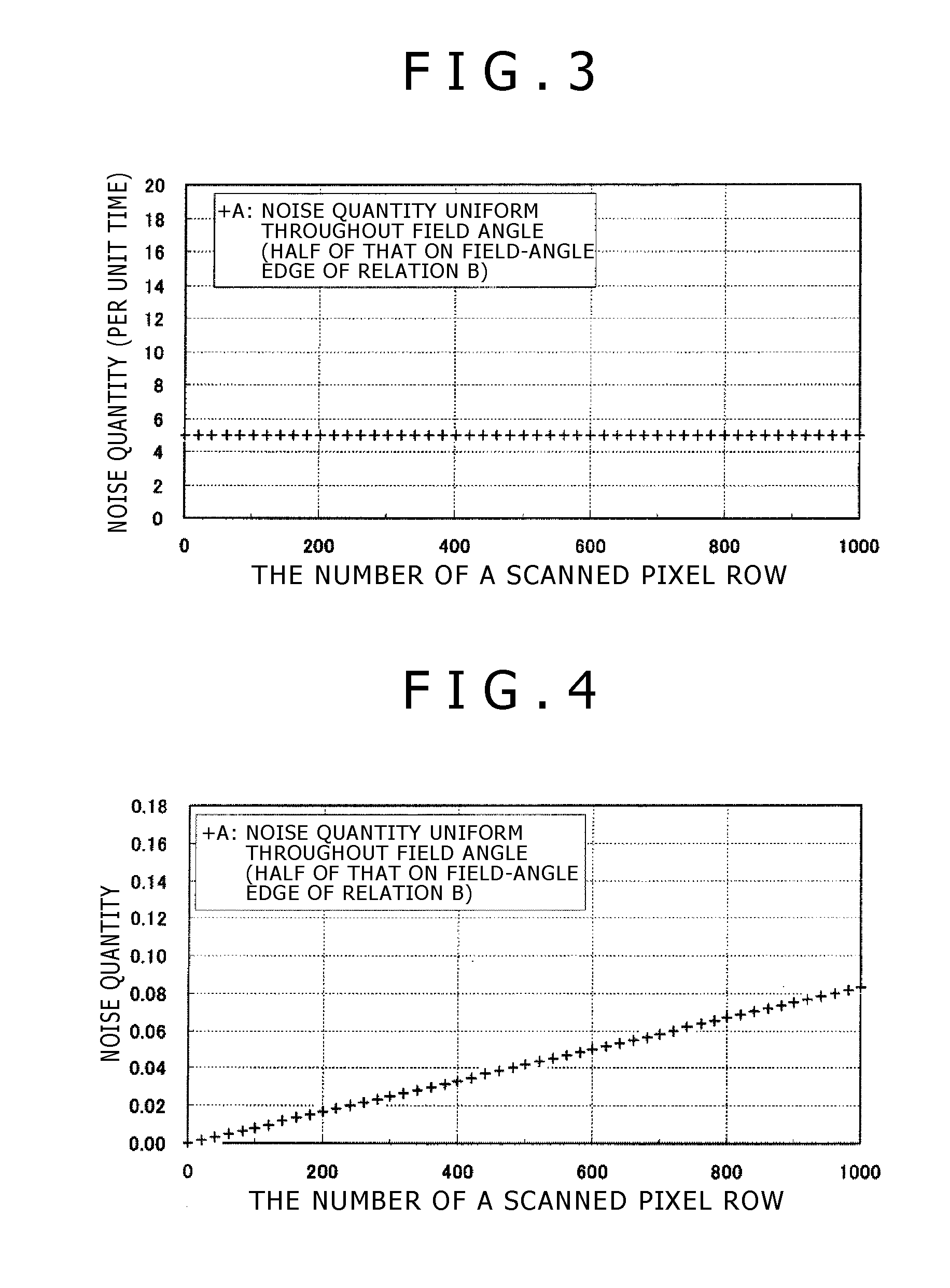
[0103]A first embodiment has been proposed on the basis of results of paying attention to the fact that unevenness of smear components is seen in the scan direction and determining causes of the unevenness. The first embodiment of the present invention is an embodiment implementing an internal layout structure adopted by a unit pixel to serve as a structure capable of reducing smear components uniformly and sufficiently throughout all unit pixels.
[0104]First of all, the following description explains the results of determining the causes of the unevenness seen in the scan direction as the unevenness of smear components. Then, as a typical application of the present invention, the following description explains a CMOS image sensor including countermeasures taken by the first embodiment in the form of the internal layout structure of the unit pixel.
Noise Unevenness in the Scan Direction
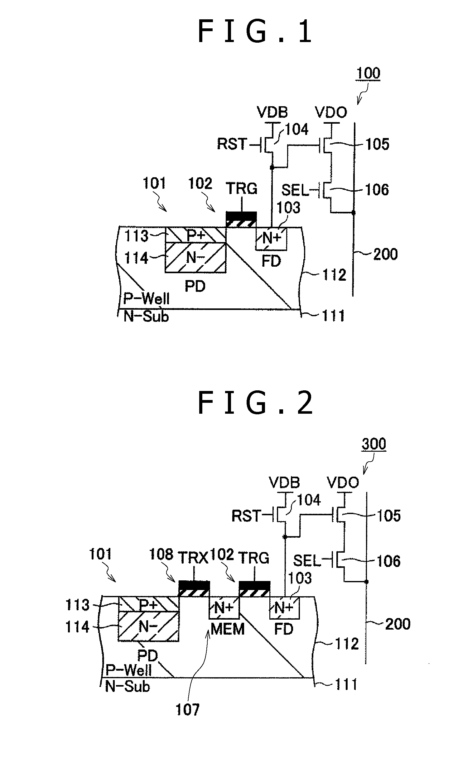
[0105]A global shutter driving operation is carried out in a pixel structure incl...
second embodiment
2: Second Embodiment
[0213]FIG. 20 is a pixel structure cross-sectional diagram referred to in the following description of a method for prescribing distances in accordance with the second embodiment. FIG. 20 is a diagram corresponding to FIG. 17 provided for the first embodiment. That is to say, FIG. 20 is a cross-sectional diagram showing a structure along a line A-B shown in FIG. 16. It is to be noted that FIGS. 10 to 16 provided for the first embodiment can also be applied to the second embodiment.
[0214]Much like FIG. 17, FIG. 20 shows a unit pixel on the ith pixel row at the center of the figure, a portion of a unit pixel on the (i−1)th pixel row on the right side of the figure and a portion of a unit pixel on the (i+1)th pixel row on the left side of the figure. The unit pixels are separated and insulated electrically from each other by an element separation layer prescribing an active layer mentioned before. In the structure shown in the figure, the element separation layer is...
third embodiment
3: Third Embodiment
[0218]FIG. 21 is a pixel structure cross-sectional diagram referred to in the following description of a method for prescribing distances in accordance with a third embodiment. FIG. 21 is a diagram corresponding to FIG. 17 provided for the first embodiment. That is to say, FIG. 21 is a cross-sectional diagram showing a structure along a line A-B shown in FIG. 16. It is to be noted that FIGS. 10 to 16 provided for the first embodiment can also be applied to the third embodiment.
[0219]Much like FIG. 17, FIG. 21 shows a unit pixel on the ith pixel row at the center of the figure, a portion of a unit pixel on the (i−1)th pixel row on the right side of the figure and a portion of a unit pixel on the (i+1)th pixel row on the left side of the figure. The unit pixels are separated and insulated electrically from each other by an element separation layer prescribing an active layer mentioned before. In the structure shown in the figure, the element separation layer is a LO...
PUM
 Abstract
Description
Claims
Application Information
 - R&D
- Intellectual Property
- Life Sciences
- Materials
- Tech Scout
- Unparalleled Data Quality
- Higher Quality Content
- 60% Fewer Hallucinations
Browse by: Latest US Patents, China's latest patents, Technical Efficacy Thesaurus, Application Domain, Technology Topic, Popular Technical Reports.
© 2025 PatSnap. All rights reserved.Legal|Privacy policy|Modern Slavery Act Transparency Statement|Sitemap|About US| Contact US: help@patsnap.com