Photoelectric conversion device and photoelectric conversion device module

a conversion device and photoelectric technology, applied in the direction of pv power plants, sustainable manufacturing/processing, final product manufacturing, etc., can solve the problems increasing the difficulty of avoiding the lowering of the conversion efficiency accompanying the area increase, and increasing the difficulty of effectively collecting electrons arising from photoelectric conversion by the photoelectric conversion layer. , to achieve the effect of increasing the thickness of the collector layer, improving the current collection efficiency, and simple structur

Inactive Publication Date: 2011-10-06
SONY CORP
View PDF2 Cites 17 Cited by
  • Summary
  • Abstract
  • Description
  • Claims
  • Application Information

AI Technical Summary

Benefits of technology

[0018]According to the first embodiment of the present invention, the photoelectric conversion device has the first substrate, the collector layer provided over this first substrate, the second substrate that is opposed to the planar surface of the first substrate and is formed of a metal having the concave notch part at one side, and the connection terminal connected to the collector layer, and the connection terminal is disposed opposed to the concave notch part. Therefore, the photoelectric conversion device has a simple structure and allows increase in the thickness of the collector layer and enhancement in the current collection efficiency. Furthermore, it is possible to provide such a photoelectric conversion device that the plural photoelectric conversion devices can be disposed in a plane in substantially close to each other and be easily mutually connected.
[0019]According to the second embodiment of the present invention, a plurality of the above-described photoelectric conversion devices are disposed in a plane, and the connection terminal of one of two photoelectric conversion devices adjacent to each other and the second substrate of the other are electrically connected to each other. Therefore, the plural photoelectric conversion devices that have a simple structure and allow enhancement in the conversion efficiency can be disposed in a plane in substantially close to each other and be easily mutually connected, and it is possible to provide a photoelectric conversion device module having an increased ratio of the light reception area to the total area of the arrangement of the plural photoelectric conversion devices and enhanced light collection efficiency.

Problems solved by technology

However, because the resistance of the transparent electrically-conductive layer of e.g. ITO or FTO is high, it is difficult to avoid the lowering of the conversion efficiency accompanying the area increase.
However, because the transparent electrically-conductive layer is required to have transparency, decreasing its resistance is subjected to certain constraints.
Therefore, as the area of the dye-sensitized solar cell becomes larger, it becomes more difficult to effectively collect electrons arising from photoelectric conversion by the photoelectric conversion layer.
As a result, the lowering of the conversion efficiency is caused due to resistive loss by the electrolyte layer.
Although dye-sensitized solar cells having a structure in which the distance between the working electrode and the opposing electrode is shortened have been reported in Patent Document 5 and Patent Document 6, this structure is complex.
However, in the solar cell modules described in Patent Document 7 and Patent Document 8, sufficient considerations for these requirements are not made.

Method used


Image

  • Photoelectric conversion device and photoelectric conversion device module
  • Photoelectric conversion device and photoelectric conversion device module
  • Photoelectric conversion device and photoelectric conversion device module

Examples


embodiment

Opposed Cell

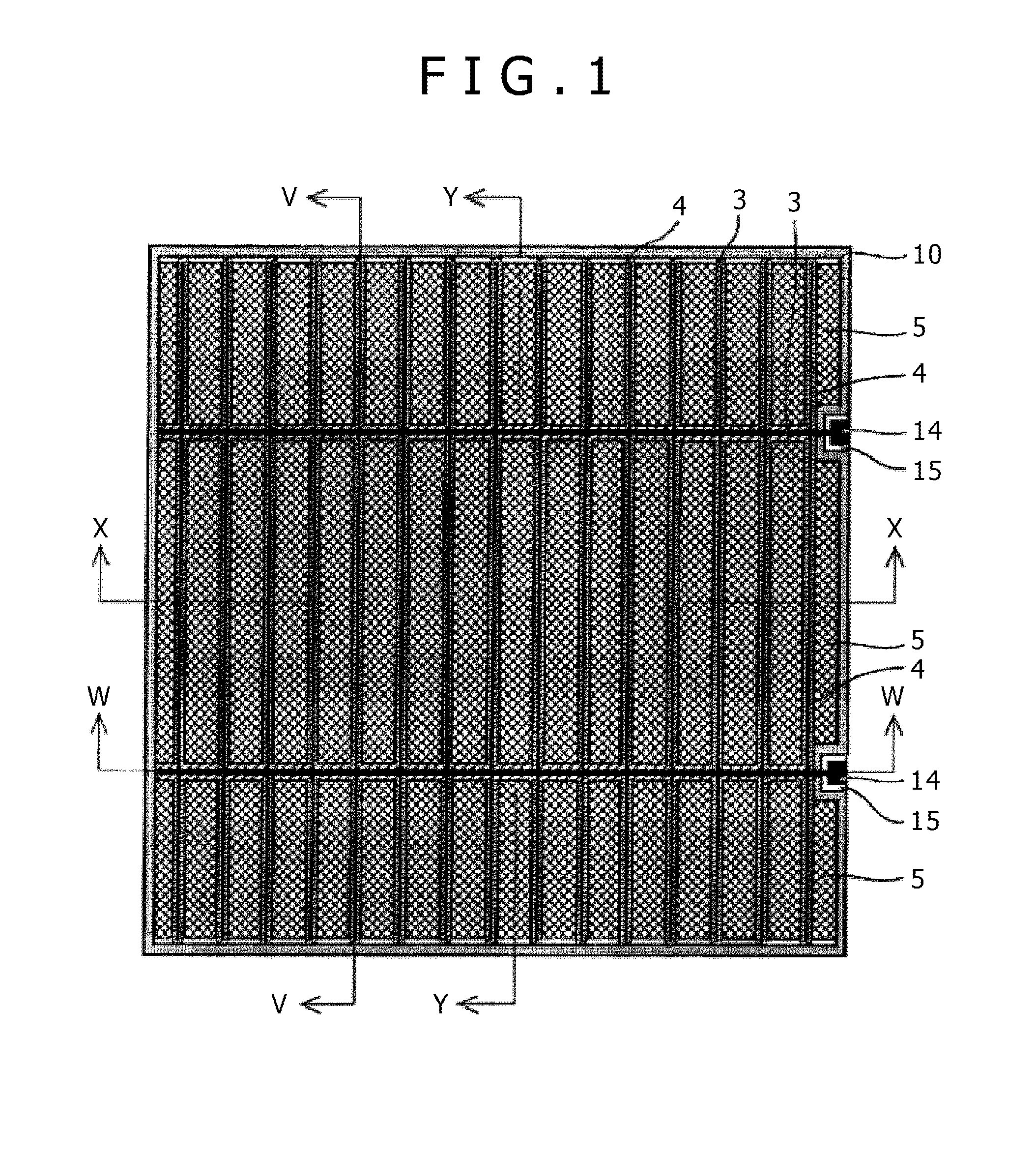
[0047]FIG. 1 is a plan view for explaining the configuration of a dye-sensitized solar cell (opposed cell) in the embodiment of the present invention.

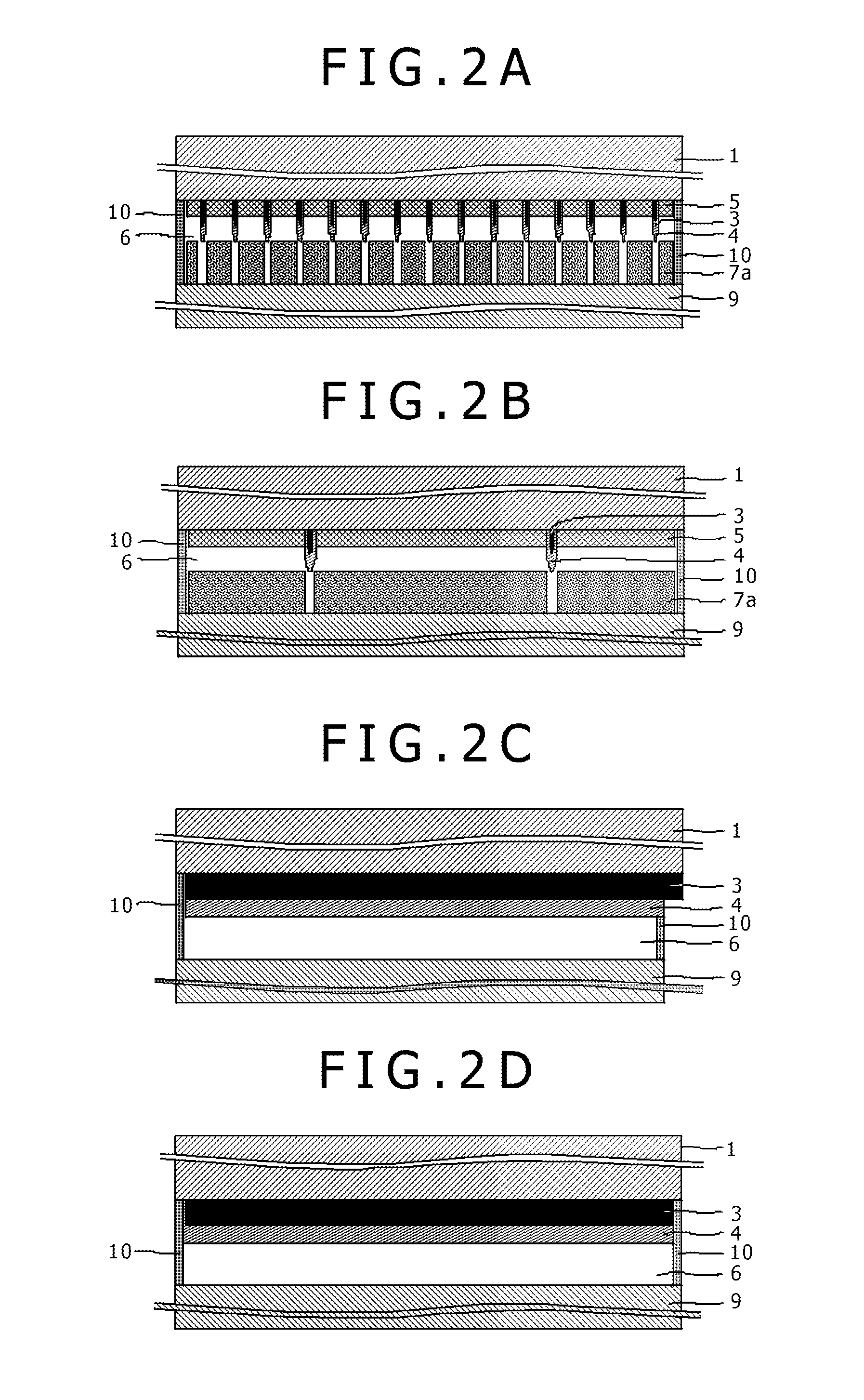
[0048]FIGS. 2A to 2D are sectional views for explaining the configuration of the dye-sensitized solar cell (opposed cell) in the embodiment of the present invention.

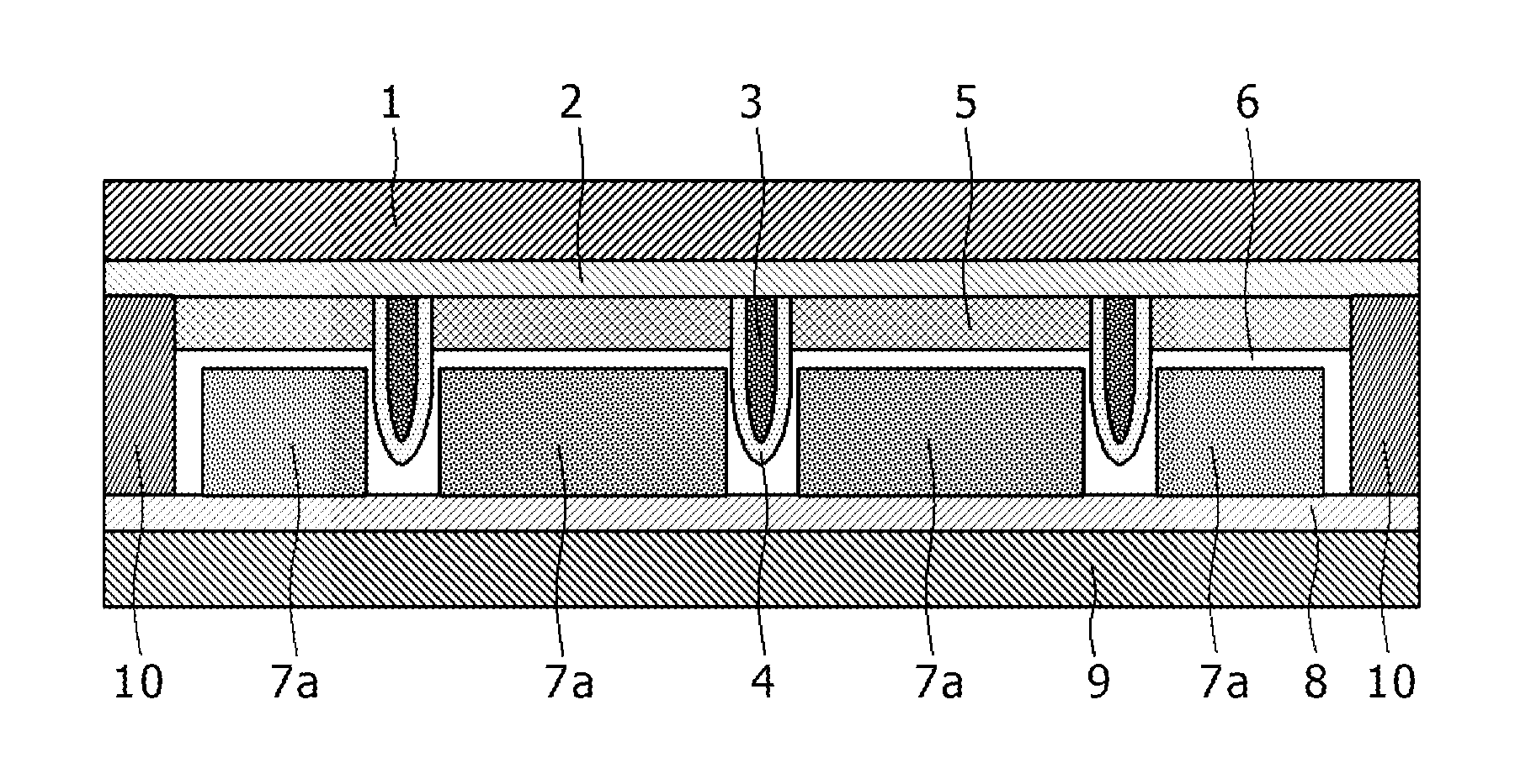
[0049]FIG. 2A is a sectional view along line X-X shown in FIG. 1 (X-X sectional view). FIG. 2B is a sectional view along line Y-Y shown in FIG. 1 (Y-Y sectional view). FIG. 2C is a sectional view along line W-W shown in FIG. 1 (W-W sectional view). FIG. 2D is a sectional view along line V-V shown in FIG. 1 (V-V sectional view).

[0050]As shown in FIG. 1 and FIGS. 2A to 2D, the opposed cell is composed of a window electrode (working electrode) on which light is incident, a counter electrode disposed opposed to the window electrode, and an electrolyte layer 6 disposed between the window electrode (working electrode) and the counter electrode. The window electrode (w...

working example

Example of Layer Configuration of Opposed Cell

[0115]Specific examples of the respective layers configuring the opposed cell shown in FIG. 1 to FIG. 3B will be described below.

[0116]FIG. 8 is a diagram for explaining the pattern of the porous photoelectric conversion layer (porous oxide semiconductor layer, TiO2 electrode) 5 in a working example of the present invention.

[0117]As shown in FIG. 8, the pattern of the porous photoelectric conversion layer 5 is formed with a thickness of 20 μm on a surface of the transparent substrate (transparent glass substrate (FTO glass substrate on which FTO is formed)) 1. The pattern is composed of sixteen columns and three rows of the porous photoelectric conversion layer 5 having a pattern of strips of 2.95 mm×23 mm, 2.95 mm×46 mm, 2.95 mm×19.5 mm, 2.95 mm×39 mm, 5.9 mm×23 mm, and 5.9 mm×46 mm.

[0118]FIG. 9 is a diagram for explaining the pattern of the catalyst layer (carbon electrode) in the working example of the present invention.

[0119]As shown...


PUM


Abstract

The present invention is to provide a photoelectric conversion device including: a first substrate; a collector layer configured to be provided over the first substrate; a second substrate configured to be opposed to a planar surface of the first substrate and be formed of a metal having a concave notch part at one side; and a connection terminal configured to be connected to the collector layer. The connection terminal is disposed opposed to the concave notch part.

Description

BACKGROUND OF THE INVENTION[0001]1. Field of the Invention[0002]The present invention relates to a photoelectric conversion device and a photoelectric conversion device module obtained by disposing the photoelectric conversion devices in a plane and connecting them to each other.[0003]2. Description of the Related Art[0004]In recent years, awareness of environmental protection is increasing and the importance of photovoltaic power generation is further increasing. In the dye-sensitized solar cell (DSSC), a transparent electrically-conductive layer and an oxide semiconductor layer are formed over a transparent substrate, and a dye-carrying oxide semiconductor layer (photoelectric conversion layer) obtained by making this oxide semiconductor layer carry a sensitizing dye is used as the working electrode (photoelectrode, window electrode). In addition, a redox electrolyte layer is disposed between this working electrode and the opposing electrode. In this dye-sensitized solar cell, ele...

Claims


Application Information

Patent Timeline
Patent Type & Authority Applications(United States)
IPC IPC(8): H01L31/042H01L31/0224H01L51/44
CPCH01G9/2031Y02E10/542H01G9/2081H01G9/2059Y02P70/50
Inventor MOROOKA, MASAHIROTADA, KEISHI
Owner SONY CORP
Why Eureka
Try Eureka