

Semiconductor device
a semiconductor and semiconductor technology, applied in the direction of transistors, electroluminescent light sources, electric lighting sources, etc., can solve the problems of insufficient reliability of transistors including oxide semiconductors, difficult suppression of charge trapping, and inability to keep the interface state favorable with an active layer, etc., to achieve stable electric characteristics, high reliability, and favorable electric characteristics
- Summary
- Abstract
- Description
- Claims
- Application Information
AI Technical Summary
Benefits of technology
Problems solved by technology
Method used
Image

Examples
embodiment 1
[0047]In this embodiment, an embodiment of a semiconductor device and a manufacturing method thereof will be described with reference to FIGS. 1A to 1C, FIG. 2, FIGS. 3A to 3G, FIGS. 4A to 4E, and FIGS. 5A to 5C.
Structural Example of Semiconductor Device
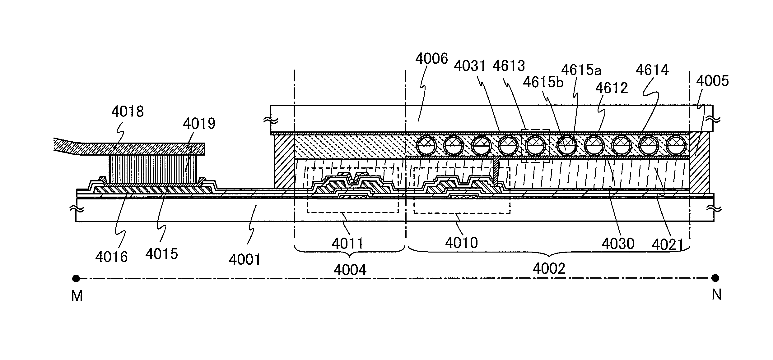
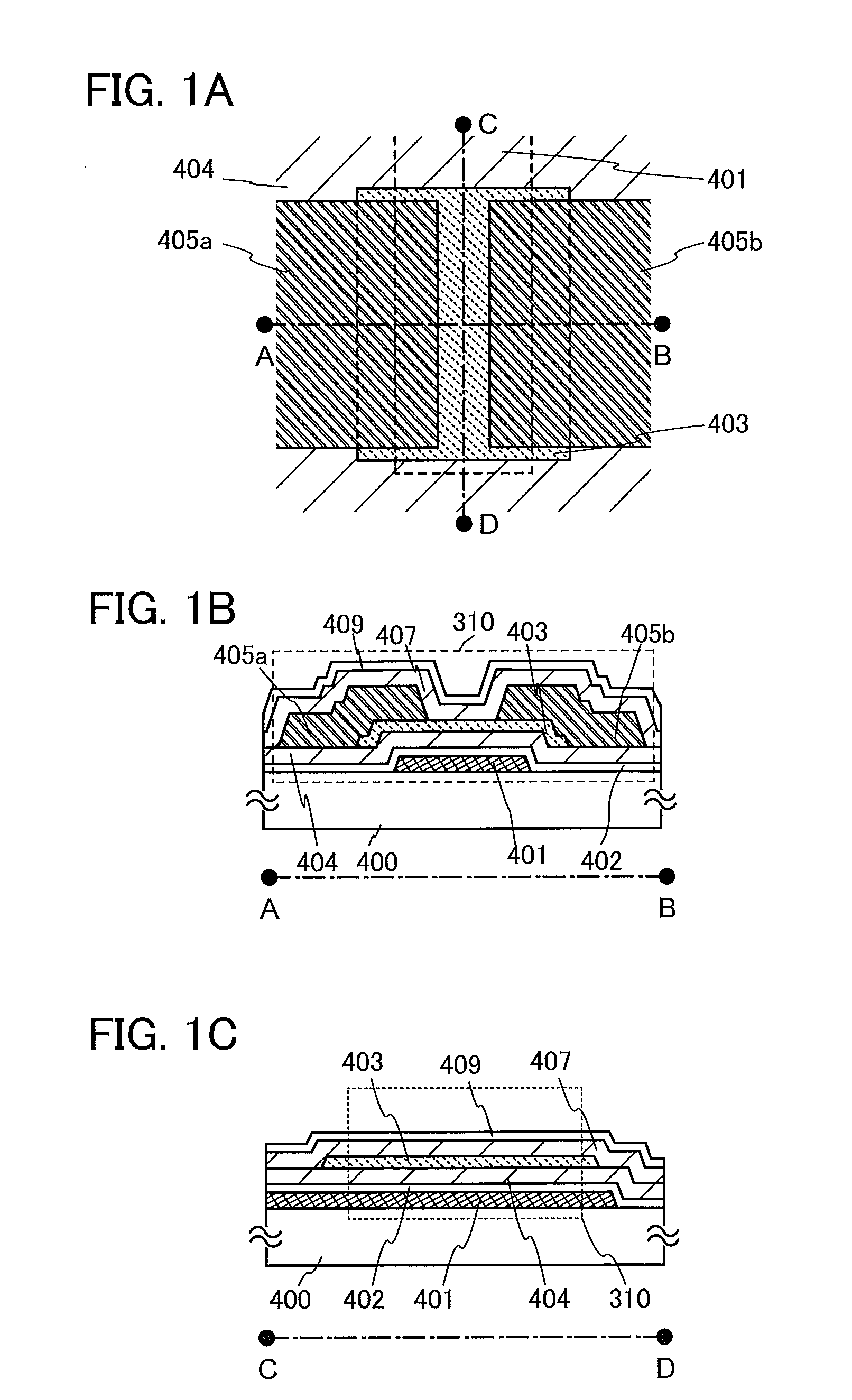
[0048]FIGS. 1A to 1C are a plan view and cross-sectional views of a bottom-gate transistor as an example of a semiconductor device. Here, FIG. 1A is a plan view, FIG. 1B is a cross-sectional view along A-B of FIG. 1A, and FIG. 1C is a cross-sectional view along C-D of FIG. 1A. Note that part of components of a transistor 310 (e.g., a second metal oxide film 407) is omitted for brevity.
[0049]The transistor 310 in FIGS. 1A to 1C includes, over a substrate 400 having an insulating surface, a gate electrode 401, a gate insulating film 402, a first metal oxide film 404, an oxide semiconductor film 403, a source electrode 405a, a drain electrode 405b, a second metal oxide film 407, and an insulating film 409.
[0050]In the transistor in FI...
embodiment 3
[0204]A semiconductor device disclosed in this specification can be applied to a variety of electronic appliances (including game machines). Examples of electronic appliances are a television set (also referred to as a television or a television receiver), a monitor of a computer or the like, a camera such as a digital camera or a digital video camera, a digital photo frame, a mobile phone handset (also referred to as a mobile phone or a mobile phone device), a portable game machine, a portable information terminal, an audio reproducing device, a large-sized game machine such as a pachinko machine, and the like. Examples of electronic appliances each including the semiconductor device described in the above embodiment are described.
[0205]FIG. 10A illustrates a laptop personal computer, which includes a main body 3001, a housing 3002, a display portion 3003, a keyboard 3004, and the like. By applying the semiconductor device described in Embodiment 1 or 2, the laptop personal compute...
PUM
 Abstract
Description
Claims
Application Information