Electro-optical device and electronic apparatus

a technology of optical devices and electronic devices, applied in electrical devices, semiconductor devices, instruments, etc., can solve the problems of light shielding property deterioration and difficulty in ensuring a high aperture ratio, and achieve the effect of high aperture ratio, narrow pitch and high accuracy of a pixel

Inactive Publication Date: 2011-10-06
SEIKO EPSON CORP
View PDF4 Cites 8 Cited by
  • Summary
  • Abstract
  • Description
  • Claims
  • Application Information

AI Technical Summary

Benefits of technology

[0006]An advantage of some aspects of the invention is that it provides an electro-optical device capable of realizing a high ap...

Problems solved by technology

In the above-described layout configuration, however, a technical problem may arise in that it is difficult to ensure a high aperture ratio while realizing the narrow pitch and the high accuracy of ...

Method used


Image

  • Electro-optical device and electronic apparatus
  • Electro-optical device and electronic apparatus
  • Electro-optical device and electronic apparatus

Examples


first embodiment

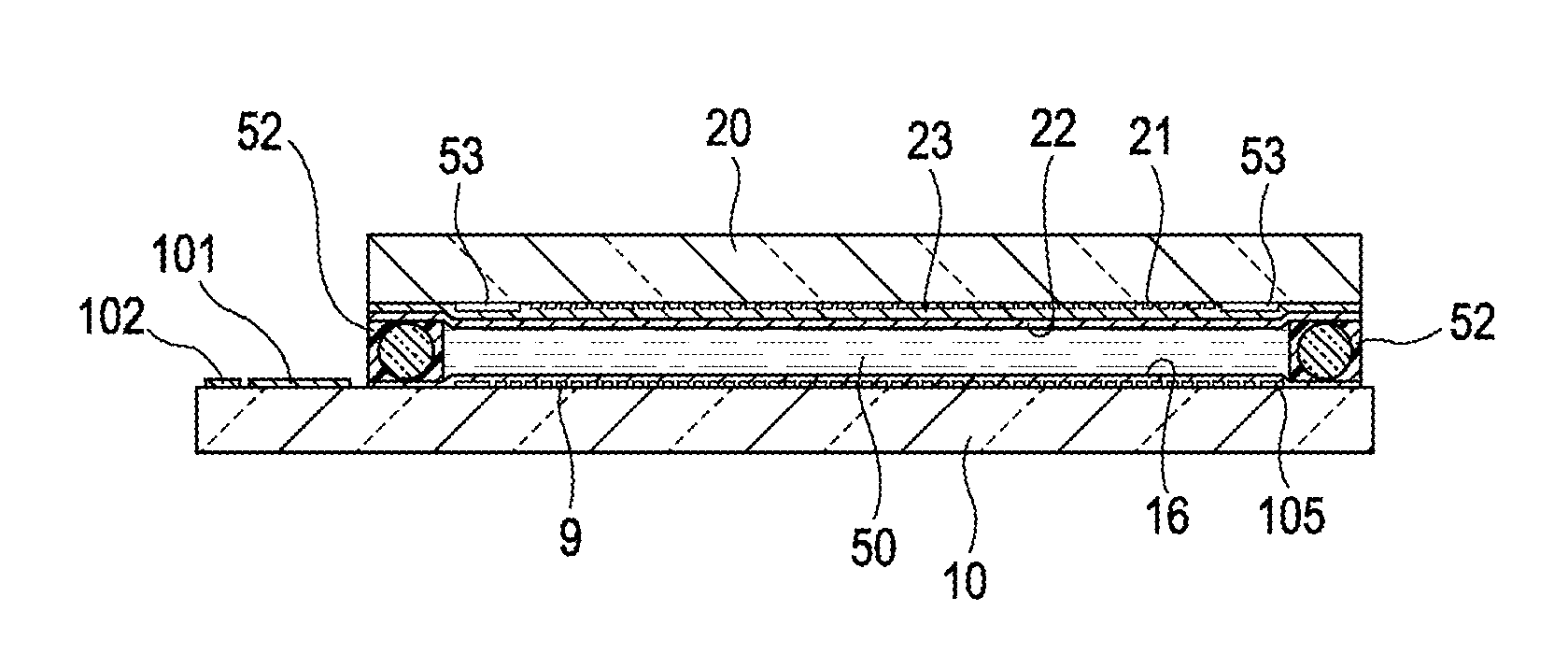
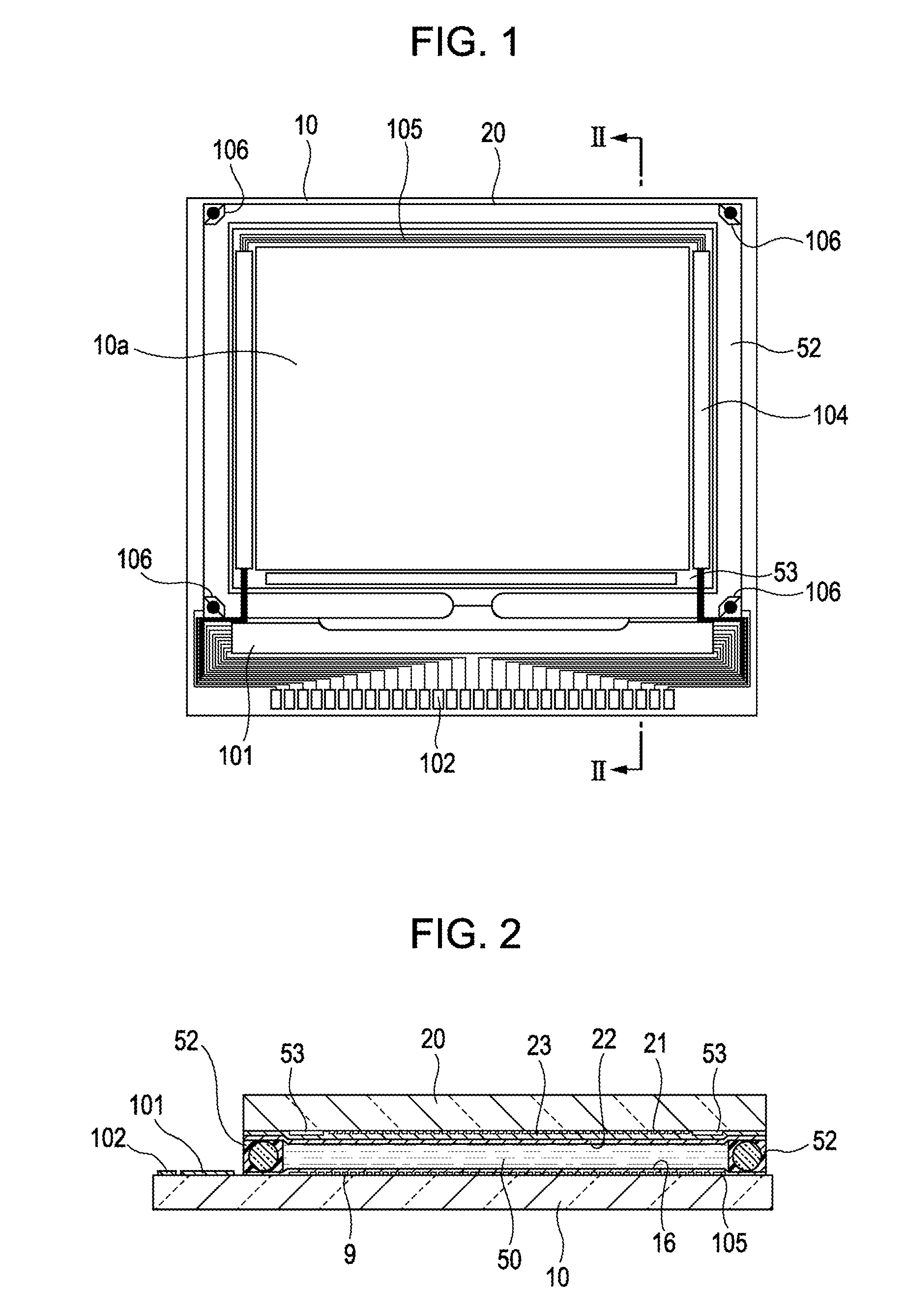
[0031]First, the entire configuration of the electro-optical device according to a first embodiment will be described with reference to FIGS. 1 and 2. FIG. 1 is a plan view illustrating the entire configuration of the electro-optical device according to this embodiment. FIG. 2 is a sectional view taken along the line II-II of FIG. 1.

[0032]In the electro-optical device according to this embodiment, as shown in FIGS. 1 and 2, a TFT array substrate 10 and a counter substrate 20 are disposed opposite to each other. The TFT array substrate 10 is an example of a “substrate” of the invention and is a transparent substrate such as a quartz substrate or a glass substrate, a silicon substrate, or the like. The counter substrate 20 is a transparent substrate such as a quartz substrate or a glass substrate. A liquid crystal layer 50 is enclosed between the TFT array substrate 10 and the counter substrate 20. The liquid crystal layer 50 includes liquid crystal in which one kind or various kinds ...

second embodiment

[0066]Next, the configuration of an electro-optical device according to a second embodiment will be described with reference to FIGS. 10 and 11. In the second embodiment, a part of the configuration of the pixel switching TFT is different from that of the first embodiment. In FIGS. 10 and 11, the same reference numerals are given to the same constituent elements as those of the first embodiment and the description thereof will not be repeated.

[0067]Hereinafter, the configuration of the pixel switching TFT 30 will be mainly described in detail according to the second embodiment. FIG. 10 is a plan view mainly illustrating an arrangement relationship between the TFT and the scanning and data lines according to the second embodiment. FIG. 11 is a sectional view taken along the line XI-XI of FIG. 10. In order to enlarge each layer and each member so as to be recognizable in the drawing, each layer and each member are appropriately shown with different scales in FIGS. 10 and 11.

[0068]In F...


PUM


Abstract

A semiconductor layer of a TFT is continuously formed from an inside of an open hole portion overlapping with an intersection up to an outside of the open hole portion and includes a first source/drain area electrically connected to a surface portion of the data line exposed to a bottom surface of the open hole portion, a channel area disposed on a side wall of the open hole portion, and a second source/drain area formed outside the open hole portion and electrically connected to the pixel electrode. The gate electrode of the TFT is formed inside the open hole portion so as to overlap with at least the channel area and is electrically connected to a scanning line.

Description

BACKGROUND[0001]1. Technical Field[0002]The present invention relates to an electro-optical device such as a liquid crystal device and an electronic apparatus including the electro-optical device.[0003]2. Related Art[0004]As an electro-optical device, JP-A-10-177190 discloses the layout configuration of the pixels in which a pixel switching transistor (TFT: Thin Film Transistor) is formed in a planar manner along a substrate surface. Specifically, the source area of the transistor is commonly used between the adjacent pixels and electric connection to data lines is made via common contacts in order to reduce a pixel pitch and achieve high accuracy (for example, see FIG. 3 or 4 in JP-A-10-177190). In this configuration, since channel areas and source and drain areas of the transistors are disposed in a plane direction along a substrate surface, current also flows in the plane direction.[0005]In the above-described layout configuration, however, a technical problem may arise in that i...

Claims


Application Information

Patent Timeline
IPC IPC(8): H01L33/08
CPCG02F1/136227H01L29/78642H01L27/1222G02F2001/13685G02F1/13685
Inventor ISHII, TATSUYA
Owner SEIKO EPSON CORP
Why Eureka
Try Eureka