Charge-pump circuit

a charge-pump circuit and circuit technology, applied in the direction of power conversion systems, instruments, dc-dc conversion, etc., can solve the problems of reducing the dickson charge-pump becomes quite unsuitable, and the circuitry is correspondingly complex, so as to improve the single-stage gain, improve the boosted output voltage, and improve the gain of the charge-pump

Active Publication Date: 2011-10-06
NXP BV
View PDF7 Cites 28 Cited by
  • Summary
  • Abstract
  • Description
  • Claims
  • Application Information

AI Technical Summary

Benefits of technology

[0015]As indicated above, using a multiple-gate transistor allows dynamic adjustment of the threshold voltage for that transistor such that the single-stage gain in a charge-pump may be improved if that stage uses a multiple-gate transistor to transfer charge. Therefore, in a particularly preferred embodiment of the invention, each transistor stage of the charge-pump circuit preferably comprises a multiple-gate transistor with a second, independently controllable gate. In such a circuit, each transistor stage has an improved single-stage gain such that the overall charge-pump circuit may deliver an improved boosted output voltage compared to prior art charge-pump circuits. In brief, such a preferred embodiment is free of the constraints due to threshold voltage considerations to which prior-art charge pump circuits are subject.
[0016]As mentioned above, recent developments in semiconductor manufacturing techniques have led to realizable multiple-gate MOSFETs. Devices with three or more independently controllable gates are conceivable. Fur the purposes of the charge-pump according to the invention, however, a second independently controllable gate is sufficient. Therefore, the multiple-gate transistor with independent gate used in the charge-pump circuit according to the invention preferably comprises a double-gate FinFET transistor such as a 4-terminal FinFET, i.e. a MOSFET having a source terminal, a drain terminal, and two gate terminals which can be controlled independently of each other. To avoid confusion, the term ‘first gate’ when used in the following is intended to refer to a gate to which a voltage is applied in order to switch the transistor on or off in the usual manner, while the terms ‘second gate’ (also called ‘independent gate’ in the following) refers to the other gate terminal, to which a voltage may be applied with the effect of increasing or decreasing the threshold voltage of the transistor.
[0017]One of the reasons for the relatively low efficiency of a conventional charge pump circuit is given by substrate losses, as will be known to the skilled person. In a further preferred embodiment of the charge-pump circuit according to the invention, therefore, the advantages of silicon-on-insulator (SOI) technology can be made use of by implementing SOI FinFET devices. Besides the advantages mentioned already, such a circuit is further characterised by a significant reduction in substrate losses, since the presence of an isolation layer, also called a “BOX” layer, in the substrate can considerably improve the efficiency of the charge-pump circuit.
[0018]In a charge-pump circuit with diode-connected transistor stages, charge is transferred from a transistor stage input to a transistor stage output if the potential at the input of a stage is greater than the potential at the output. The potential at alternate transistor stage input nodes is usually increased by applying a control voltage to those nodes. Therefore, in a particularly preferred embodiment of the invention, the first and second control voltages comprise essentially square-wave signals of opposite phase such that the potential at alternate transistor stage input nodes can be increased uniformly and rapidly.

Problems solved by technology

However, for low-voltage applications where the supply voltage is not much greater than the threshold voltage, the Dickson charge-pump becomes quite unsuitable since its single-stage gain is then negligible.
However, this type of circuit also has its limitations, namely reverse charge leakage over the charge-transfer switches, which results in a lower boosted output voltage.
To overcome this, an additional pair of transistors must be included for each boosting stage in order to completely turn off the charge-transfer switch transistors, resulting in a correspondingly complex circuitry and increased power dissipation.

Method used


Image

  • Charge-pump circuit
  • Charge-pump circuit
  • Charge-pump circuit

Examples


Embodiment Construction

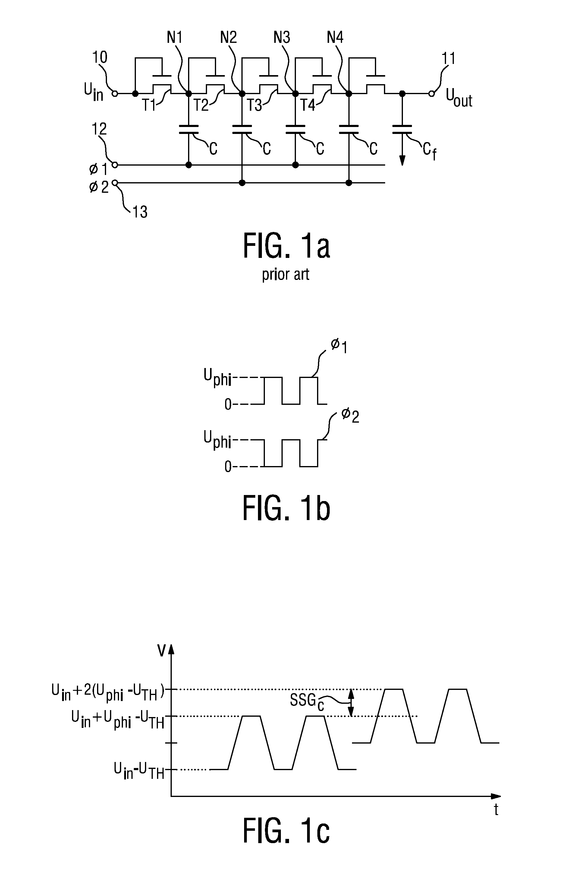
[0042]FIG. 1 shows a state-of-the-art Dickson charge-pump circuit comprising a series of transistor stages. Each transistor stage includes a transistor T1, T2, T3, T4, typically a MOSFET, whose drain is connected to the source of the transistor of the next stage and to a capacitor C, which is also connected to a control voltage node 12, 13. An input supply voltage Uin is applied at an input node 10. First and second control voltage signals Φ1, Φ2 are applied at first and second control voltage input nodes 12, 13 respectively. A capacitor Cf at the output node 11 serves to reduce the ripple on the output voltage Uout.

[0043]The output boosted voltage Uout is dependent on a number of factors, such as the number of transistor stages, the capacitance of the capacitors C, the level of the input voltage Uin and the highest level Uphi of the control voltage signals Φ1, Φ2, the frequency of the control voltage signals Φ1, Φ2 etc. The capacitors C are generally chosen to have the same value, ...


PUM


Abstract

The invention describes a charge-pump circuit (1, 1′) comprising a supply voltage input node (10) for applying an input voltage (Uin) to be boosted, a boosted voltage output node (11) for outputting a boosted voltage (Uout), and a plurality of transistor stages connected in series between the supply voltage input node (10) and the boosted voltage output node (11), wherein at least one transistor stage comprises a multiple-gate transistor (D1, . . . , D5), which transistor (D1, . . . , D5) comprises at least two gates, of which one is a first gate (G) for switching the transistor (D1, . . . , D5) on or off according to a voltage applied to the first gate (G), and one is an additional second gate (Gi) for controlling the threshold voltage of the multiple-gate transistor (D1, . . . , D5), independently of the first gate (G), according to a control voltage (Φ1, Φ2) applied to the second gate (Gi). The invention further describes a method of boosting a voltage using a charge-pump circuit (1, 1′) comprising a plurality of transistor stages connected in series between a supply voltage input node (10) and a boosted voltage output node (11), wherein at least one transistor stage comprises a multiple-gate transistor (D1, . . . , D5), which method comprises applying an input voltage (Uin) to be boosted at the supply voltage input node (10); applying a control voltage, (Φ1, Φ2) to the second gate (Gi) of the multiple-gate transistor (D1, . . . , D5) to control the threshold voltage of the multiple-gate transistor (D1, . . . , D5); and outputting the boosted voltage (Uout) at the voltage output node (11).

Description

FIELD OF THE INVENTION[0001]The invention describes a charge-pump circuit and a method of boosting a voltage using a charge-pump circuit.BACKGROUND OF THE INVENTION[0002]Charge-pumps are circuits that can pump charge upward to produce voltages higher than the regular supply voltage, using capacitors to store energy between stages. Charge is transferred from one stage to the next, usually by means of a chain of diodes. In low-voltage applications, the ‘diodes’ in the chain are generally MOSFETs (metal-oxide semiconductor field-effect transistors) connected so that charge can only flow in one direction, i.e. so that the transistors act as diodes having a certain forward bias voltage. Charge-pumps using semiconductor technology are used extensively in memories and in many power-management integrated circuits. Another important field of use of such charge-pump circuits is in passive RFID (radio-frequency identifier) tags where the AC voltage received by the tag's transceiver is first co...

Claims


Application Information

Patent Timeline
Patent Type & Authority Applications(United States)
IPC IPC(8): G05F3/02
CPCH02M3/073H02M3/07
Inventor CURATOLA, GILBERTOPONOMAREV, YOURI VICTOROVITCH
Owner NXP BV
Why Eureka
Try Eureka