Aluminum gallium nitride barriers and separate confinement heterostructure (SCH) layers for semipolar plane iii-nitride semiconductor-based light emitting diodes and laser diodes

Inactive Publication Date: 2011-10-06
RGT UNIV OF CALIFORNIA
View PDF5 Cites 35 Cited by
  • Summary
  • Abstract
  • Description
  • Claims
  • Application Information

AI Technical Summary

Benefits of technology

[0037]The present invention further discloses a method of using an Al containing barrier layer in a quantum well structure of a device, comprising usin

Problems solved by technology

Despite successful demonstration of the green LDs, the devices grown on the c-plane suffer from the Quantum Confined Stark Effect (QCSE) due to the large polarization-related electric fields, which cause lower internal quantum efficiencies due to the spatial separation of the electron and hole wave functions in the quantum wells [3].
This ma

Method used


Image

  • Aluminum gallium nitride barriers and separate confinement  heterostructure (SCH) layers for semipolar plane iii-nitride semiconductor-based light emitting diodes and laser diodes
  • Aluminum gallium nitride barriers and separate confinement  heterostructure (SCH) layers for semipolar plane iii-nitride semiconductor-based light emitting diodes and laser diodes
  • Aluminum gallium nitride barriers and separate confinement  heterostructure (SCH) layers for semipolar plane iii-nitride semiconductor-based light emitting diodes and laser diodes

Examples


Embodiment Construction

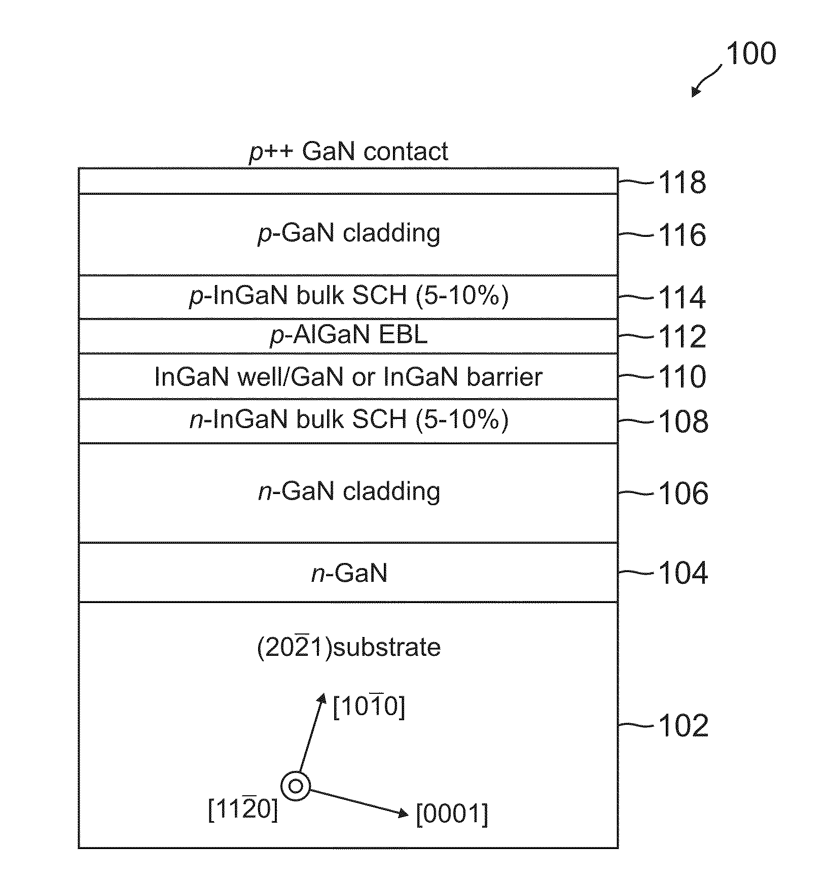
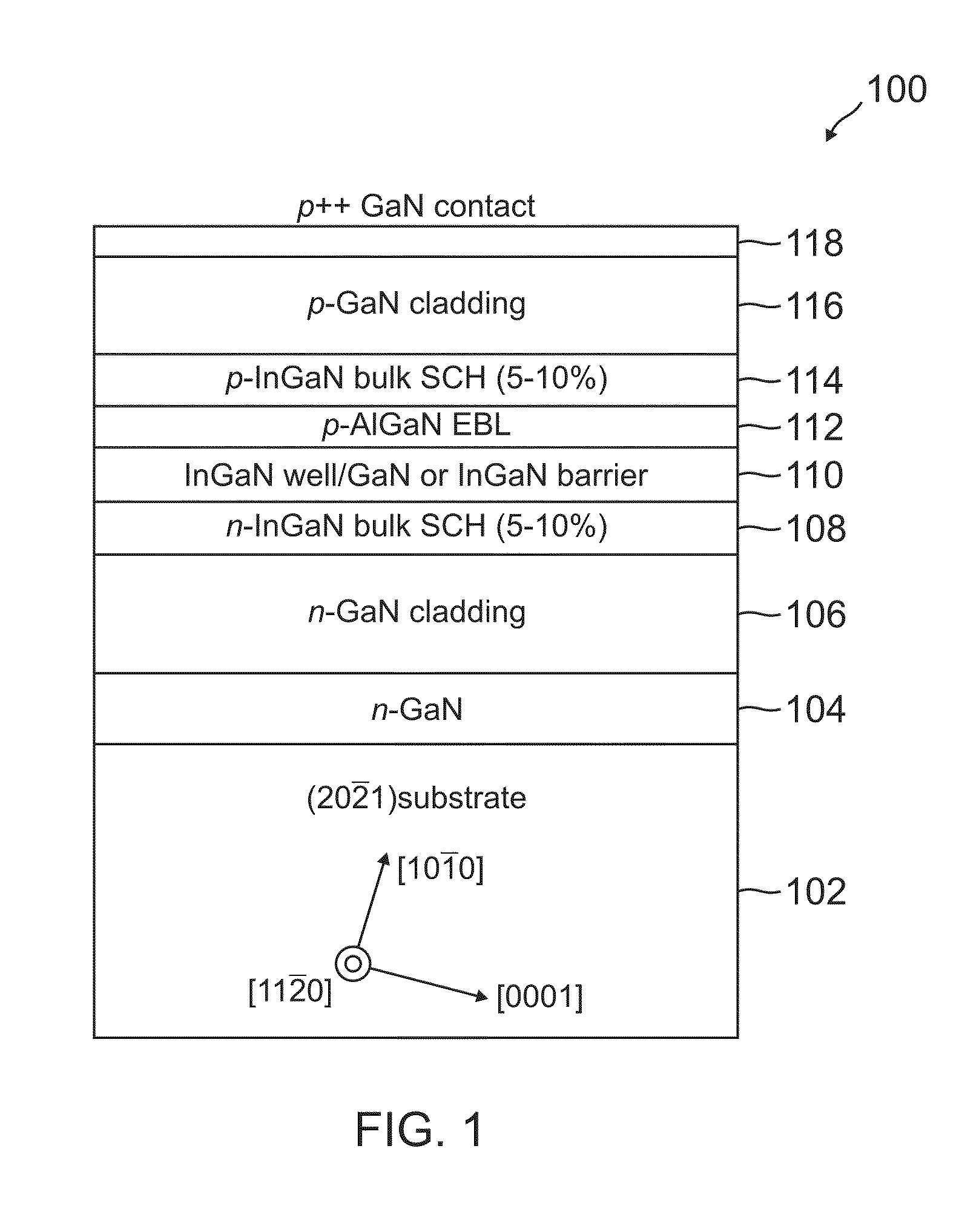
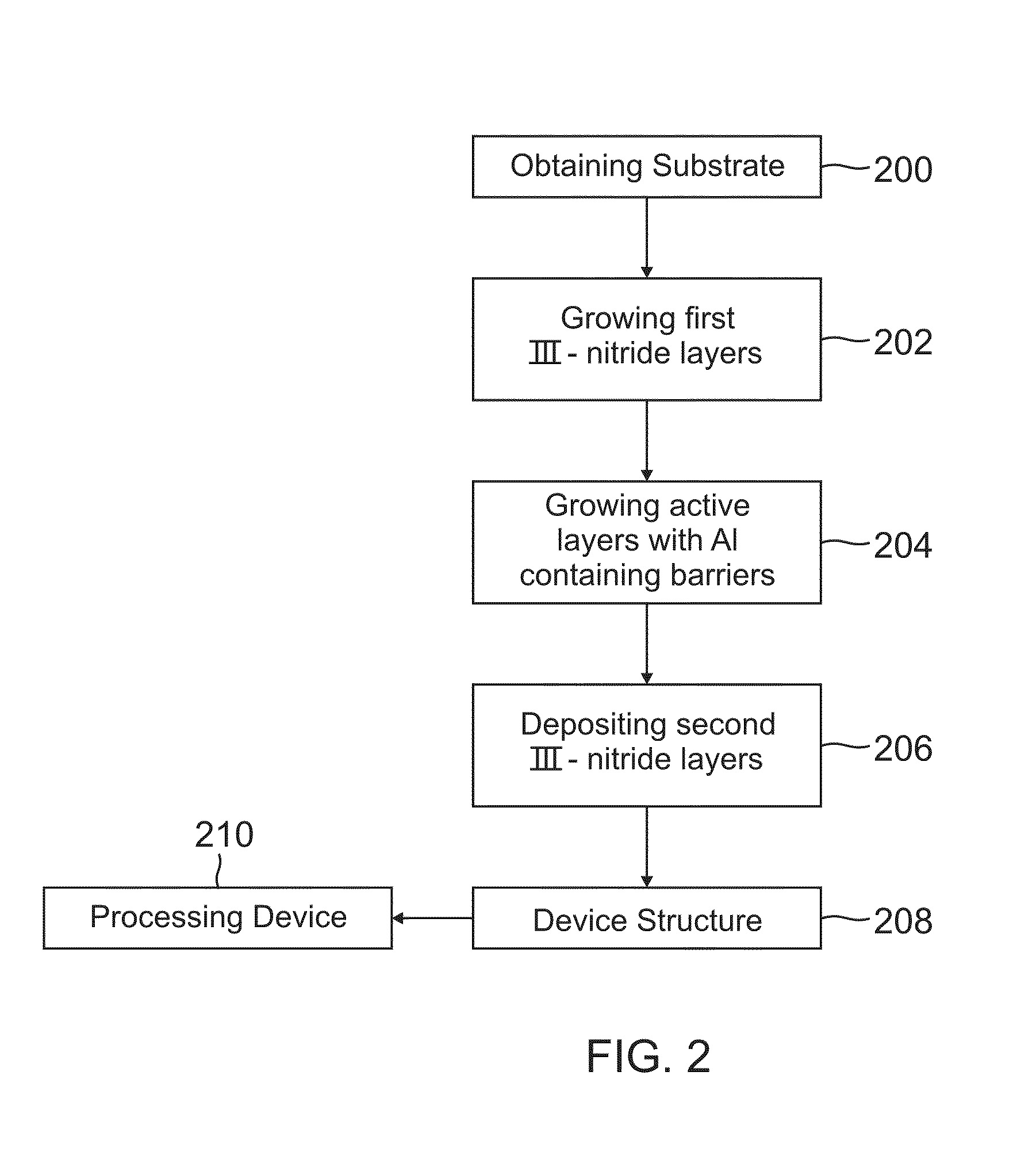
[0065]In the following description of the preferred embodiment, reference is made to the accompanying drawings which form a part hereof, and in which is shown by way of illustration a specific embodiment in which the invention may be practiced. It is to be understood that other embodiments may be utilized and structural changes may be made without departing from the scope of the present invention.

[0066]Overview

[0067]A purpose of the present invention was to develop high-efficiency semipolar (20 21)-plane LDs in the green spectral range. A goal was to achieve smooth interfaces and smooth surface morphology and reduce nonradiative defects while using high In content InGaN wells, together with a highly efficient active region, and uniform and smooth high In content InGaN superlattice SCH layers.

[0068]The use of AlGaN barriers before and between quantum wells resulted in smooth morphology (as illustrated in the fluorescence microscope images), and smooth interfaces in the laser structur...


PUM


Abstract

A semipolar plane III-nitride semiconductor-based laser diode or light emitting diode, comprising a semipolar Indium containing multiple quantum wells for emitting light, having Aluminum containing quantum well barriers, wherein the Indium containing multiple quantum well and Aluminum containing barriers are grown in a semipolar orientation on a semipolar plane.

Description

CROSS REFERENCE TO RELATED APPLICATIONS[0001]This application claims the benefit under 35 U.S.C. Section 119(e) of co-pending and commonly assigned U.S. Provisional Patent Application Ser. No. 61 / 320,954, filed on Apr. 5, 2010, by You-Da Lin, Hiroaki Ohta, Shuji Nakamura, Steven P. DenBaars and James S. Speck, entitled “AlGaN BARRIERS AND SEPARATE CONFINEMENT HETEROSTRUCTURE (SCH) LAYERS FOR SEMIPOLAR PLANE III-NITRIDE SEMICONDUCTOR-BASED LIGHT EMITTING DIODES AND LASER DIODES,” attorney's docket number 30794.367-US-P1 (2010-544-1);[0002]which application is incorporated by reference herein.[0003]This application is related to the following co-pending and commonly-assigned U.S. patent applications:[0004]U.S. Utility patent application Ser. No. 12 / 030,117, filed on Feb. 12, 2008, by Daniel F. Feezell, Mathew C. Schmidt, Kwang Choong Kim, Robert M. Farrell, Daniel A. Cohen, James S. Speck, Steven P. DenBaars, and Shuji Nakamura, entitled “Al(x)Ga(1-x)N-CLADDING-FREE NONPOLAR GAN-BASED...

Claims


Application Information

Patent Timeline
IPC IPC(8): H01S5/343H01L33/06
CPCB82Y20/00H01L33/06H01L33/16H01L33/32H01S2304/04H01S5/3202H01S5/3406H01S5/342H01S5/34333H01S5/3063H01S5/320275H01S5/2009H01S5/2031H01S5/34
Inventor LIN, YOU-DAOHTA, HIROAKINAKAMURA, SHUJIDENBAARS, STEVEN P.SPECK, JAMES S.
Owner RGT UNIV OF CALIFORNIA
Why Eureka
Try Eureka