Segmented distributed feedback laser

a distributed feedback and laser technology, applied in semiconductor lasers, instruments, optical elements, etc., can solve the problems of long distance systems, limited capacity, and non-ideal large-scale photonic integration, and achieve the effect of narrow linewidth and low power consumption

Active Publication Date: 2011-10-06
INFINERA CORP
View PDF5 Cites 12 Cited by
  • Summary
  • Abstract
  • Description
  • Claims
  • Application Information

AI Technical Summary

Problems solved by technology

Such long-distance systems, e.g. having optical fiber spans greater than 80 km, are limited in capacity by the optical channel spacing of carrier wavelengths and by the modulation format utilized.
However, to transmit and receive sufficiently error-free data under these conditions, a sufficiently narrow linewidth laser source is often used.
While all of these laser sources offer significant attributes, each has one or more deficiencies which make them non-ideal for large-scale photonic integration, such as part of PIC device for example.
For example, external-feedback lasers, by design, are incapable of monolithic integration.
DFB lasers must be excessively large to achieve narrow linewidth, and thus consume large amounts of power and require a correspondingly large area of the integrated circuit, area which could be used for other components or for additional devices as part of a fabricated wafer to increase overall yield.
Additionally, such long DFB lasers result in an exponential increase in energy at the center of the laser cavity resulting in spatial hole burning and gain loss with respect to the fundamental mode of the laser if the grating coupling strength is not adjusted.
DBR lasers are susceptible to mode-hopping, for example jumping from one longitudinal mode to another due to operating conditions such as temperature, and require complex tuning algorithms with 3 or more sections contacted to have stable operation over life.
Photonic bandgap lasers fabricated to date require cleaves and / or suffer from unpredictable yield, and therefore are unsuitable for large-scale photonic integration.

Method used


Image

  • Segmented distributed feedback laser
  • Segmented distributed feedback laser
  • Segmented distributed feedback laser

Examples


Embodiment Construction

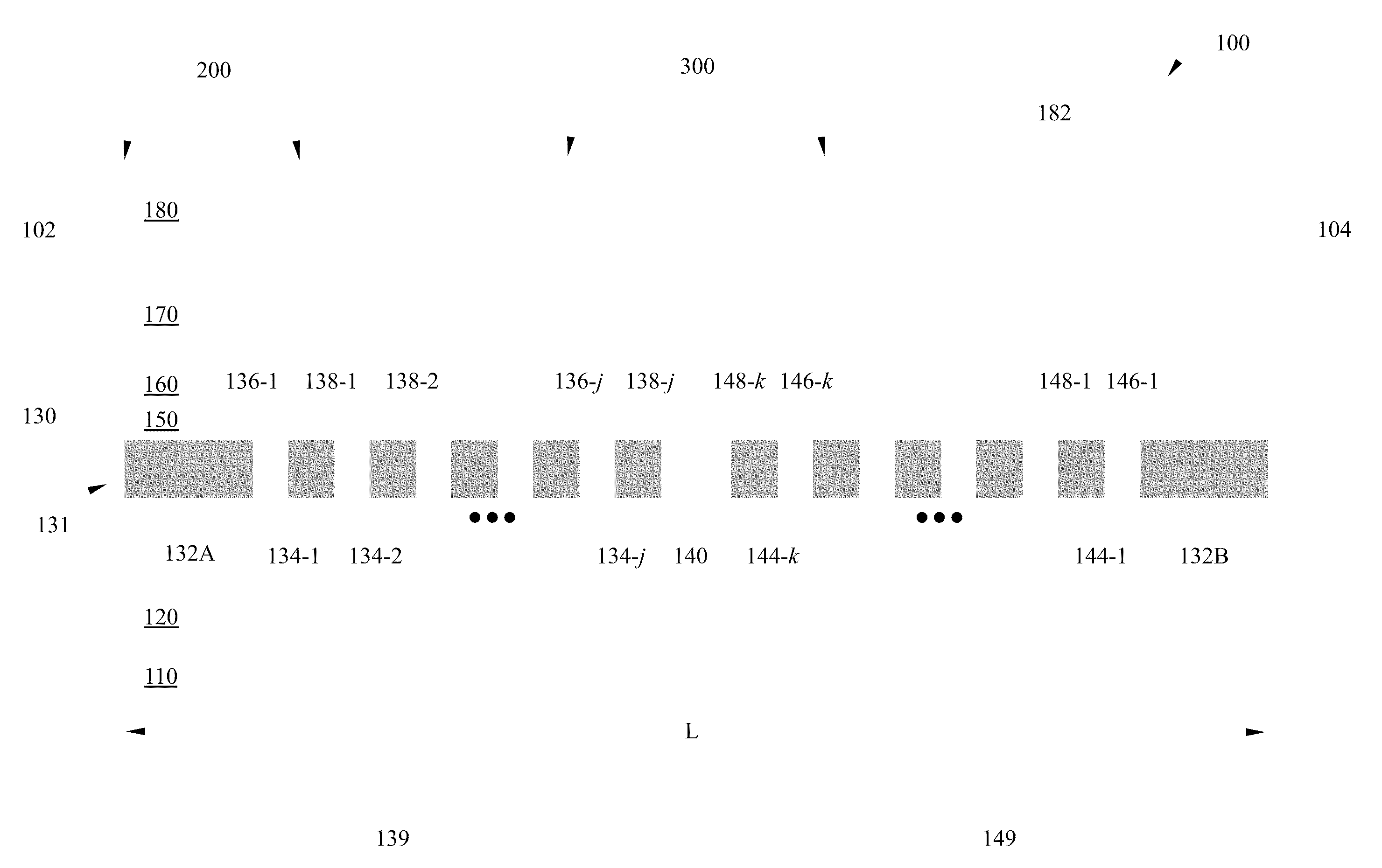
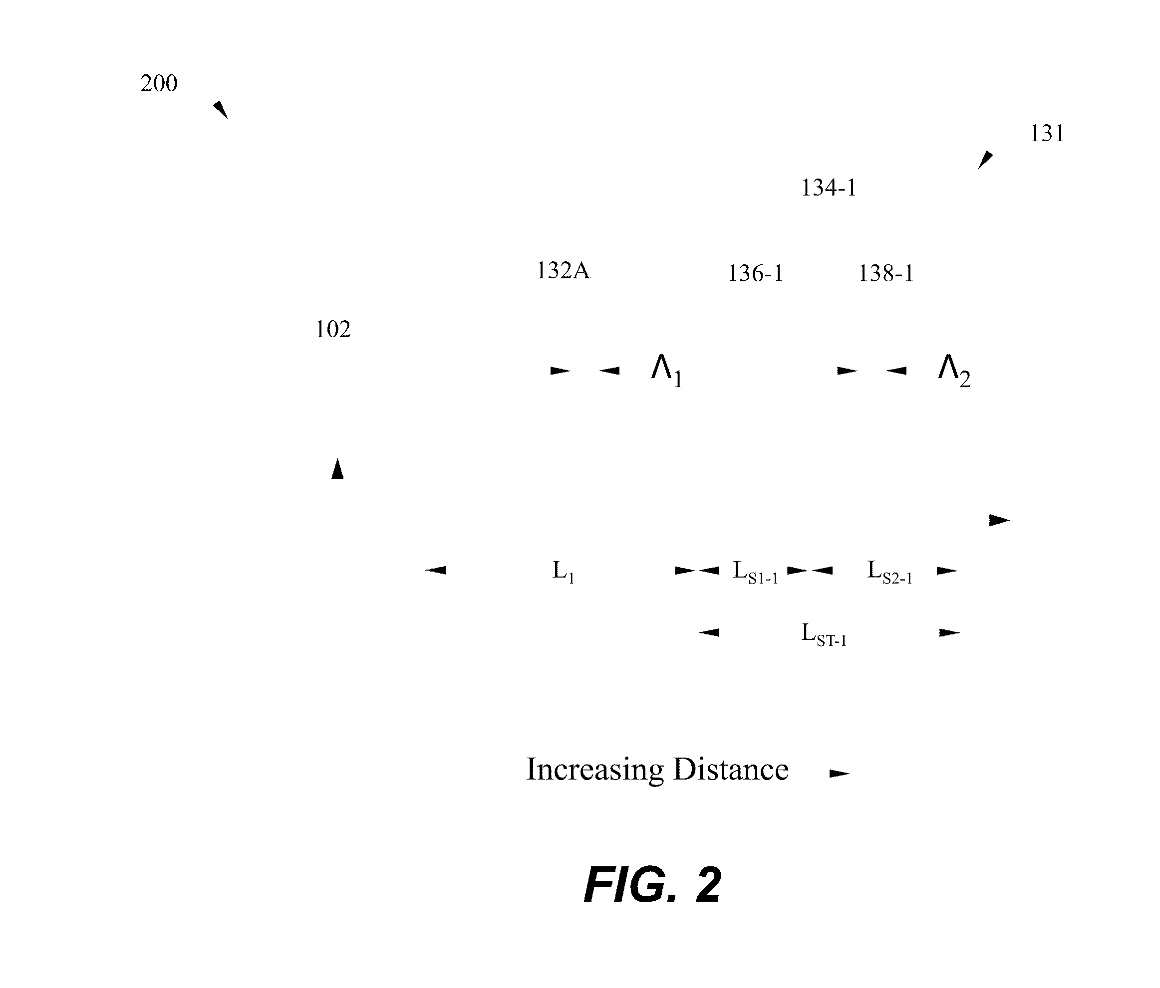
The present invention provides a system, apparatus and method to provide a semiconductor laser having a narrow linewidth and low power consumption for optical communication applications. According to various embodiments of the invention, the semiconductor laser preferably includes a grating layer comprising a plurality of segmented gratings, each including a non-grating portion and a grating portion. The segmented gratings are configured to enhance a fundamental mode of the semiconductor laser while sufficiently suppressing modes other than the fundamental mode, such that a relatively narrow linewidth more suited for high-speed data transmission in an optical communication network can be achieved, for example. The segmented gratings are also configured to provide a longer effective length of a semiconductor laser, which allows for smaller device areas and corresponding lower power consumption, as well as overall higher yields. For purposes herein, the effective length of the laser m...


PUM


Abstract

The present invention provides for a semiconductor laser having a narrow linewidth and low power consumption for optical communication applications. According to various embodiments of the invention, a semiconductor laser is provided which includes a grating layer comprising a plurality of segmented gratings, each including a non-grating portion and a grating portion. The segmented gratings are configured to enhance a fundamental mode of the semiconductor laser while sufficiently suppressing modes other than the fundamental mode, providing a narrow linewidth for example. The segmented gratings are also configured to provide an effective length longer than an actual length of the semiconductor laser, leading to smaller device areas and corresponding lower power consumption. A photonic integrated circuit is also provided which includes a plurality of semiconductor lasers, consistent with the present invention, as well as additional optical elements, all provided on a single substrate.

Description

BACKGROUND OF THE INVENTION1. Field of the InventionThis invention relates generally to semiconductor lasers and, more particularly, to grating structures within semiconductor lasers.2. Description of the Related ArtThe use of compact photonic integrated circuits (PICs) has become widespread as the need for long-distance high-speed telecommunication systems has grown. Such long-distance systems, e.g. having optical fiber spans greater than 80 km, are limited in capacity by the optical channel spacing of carrier wavelengths and by the modulation format utilized. On-Off keying (OOK) modulation formats, for example, interact strongly with optical fiber nonlinearities to be useful at high data rates and close channel spacings. Accordingly, to maximize system throughput, phase modulation formats, such as differential quadrature phase shift keying (DQPSK) or differential phase shift keying (DPSK) for example, or polarization multiplexed versions of such formats, such as polarization multi...

Claims


Application Information

Patent Timeline
Patent Type & Authority Applications(United States)
IPC IPC(8): H01S5/323H01S5/026G02B6/34H01L21/20G02B27/44H01S5/12
CPCH01S5/1039H01S5/1209H01S5/1206H01S5/12H01S5/1215
Inventor EVANS, PETER W.CORZINE, SCOTT
Owner INFINERA CORP
Why Eureka
Try Eureka