Method And Circuit To Generate Race Condition Test Data At Multiple Supply Voltages

a technology of race condition and test data, applied in the field of method and circuit for characterizing the process variation of the semiconductor die, can solve the problems of circuit failure, large random time variation, and low power design yield loss, and achieve the effect of improving the method of measuring and characterizing process variation

Inactive Publication Date: 2011-10-06
QUALCOMM INC
View PDF12 Cites 13 Cited by
  • Summary
  • Abstract
  • Description
  • Claims
  • Application Information

AI Technical Summary

Benefits of technology

[0008]One particular advantage provided by at least one of the disclosed embodiments is that an approximate supply voltage level at which a race condition occurs may be detected and used to derive or characterize local process variation. Thus, an enhanced method of measuring and characterizing process variation is provided.

Problems solved by technology

However, small transistors and reduced supply voltages lead to larger random time variations.
When large random time variations occur, circuits may fail.
Local random process variation is one of the causes of timing failure.
Large local random process variation can cause yield loss for low power designs.
However, when process variation and supply voltage variation are present, the clock path may become faster than the data path.

Method used


Image

  •  Method And Circuit To Generate Race Condition Test Data At Multiple Supply Voltages
  •  Method And Circuit To Generate Race Condition Test Data At Multiple Supply Voltages
  •  Method And Circuit To Generate Race Condition Test Data At Multiple Supply Voltages

Examples


Embodiment Construction

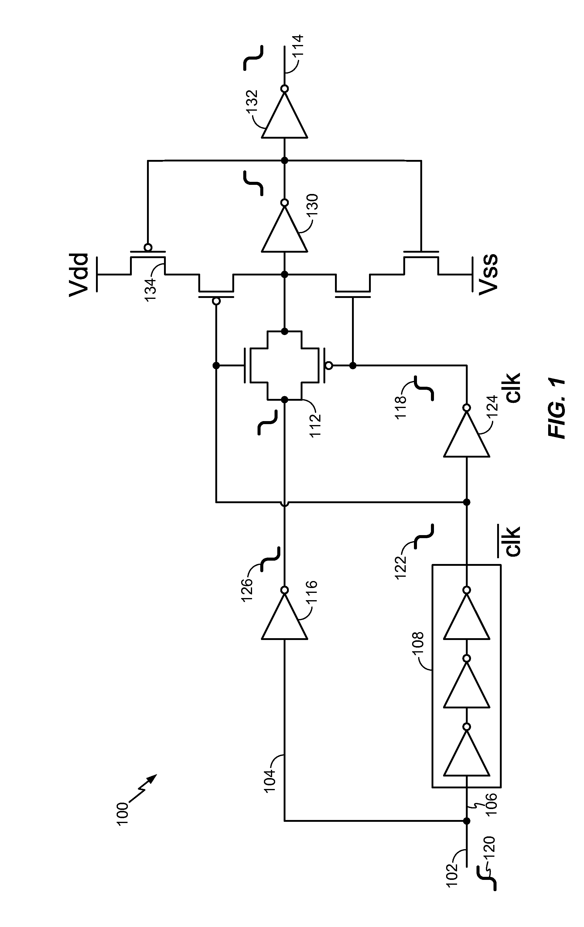
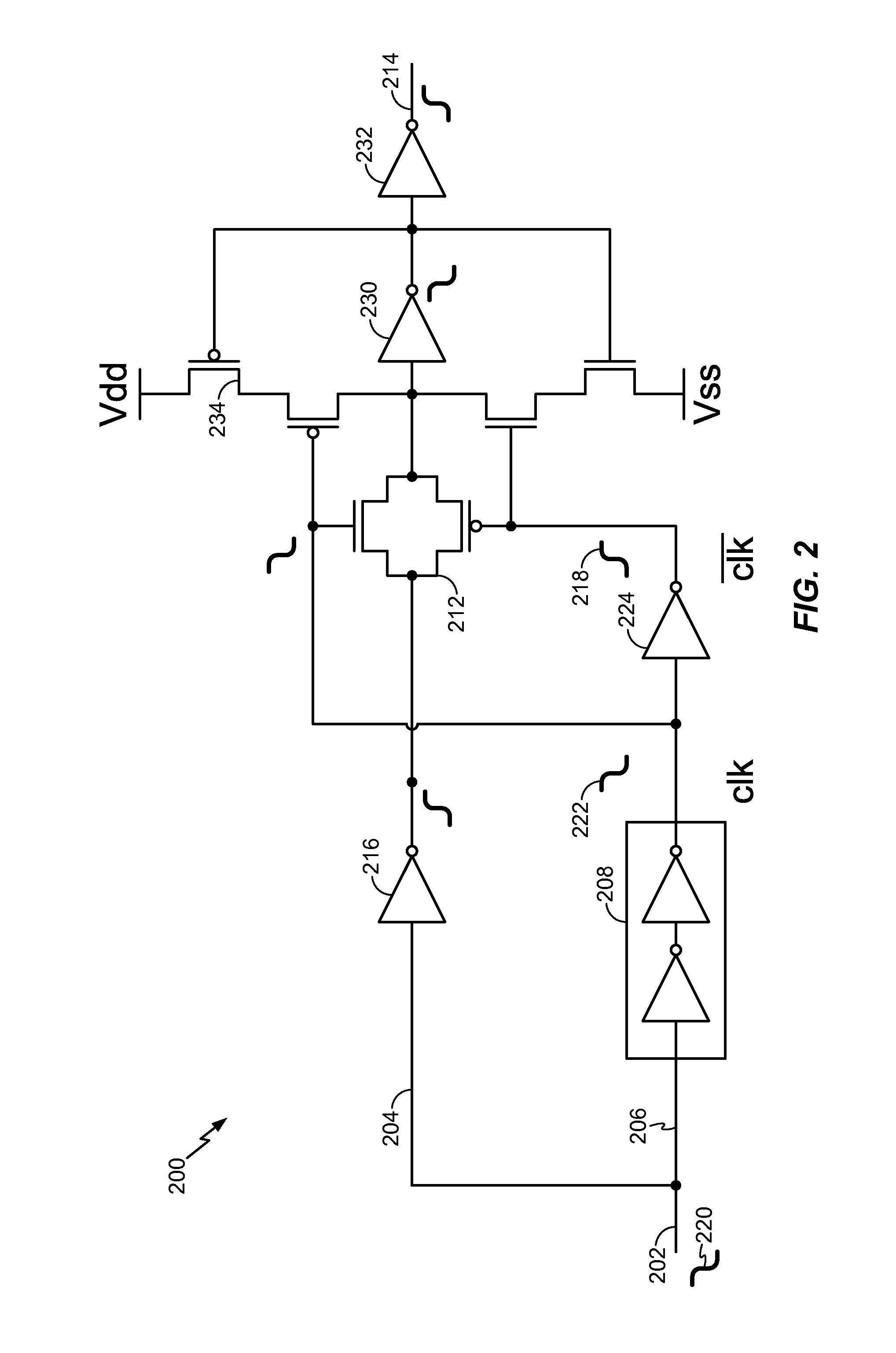
[0025]Referring to FIG. 1, a particular illustrative embodiment of a circuit is illustrated. The circuit includes a racing path circuit 100 as illustrated. The racing path circuit 100 includes a first path 104 and a second path 106. The first path 104 includes at least one delay element such as gate delay element 116. The second path 106 includes multiple delay elements. For example, the second path 106 includes multiple gate delay elements within delay circuitry 108. In a particular illustrative embodiment, the second path 106 includes at least one more gate delay element than the first path 104. For example, the second path 106 may include two gate delay circuits within the delay circuitry 108, whereas the first path 104 includes a single gate delay element 116. The gate delay element 116 and the gate delay elements contained within the delay circuitry 108 may include an inverter, a non-inverting buffer, or any other type of delay element configured to delay a signal sent over the...


PUM


Abstract

A method and circuit for characterizing a process variation of a semiconductor die is disclosed. In a particular embodiment, the method includes operating a circuit at multiple supply voltage levels to generate race condition testing data. The circuit is disposed on at least one die of a wafer and includes at least one racing path circuit having at least two paths. The method further includes collecting the race condition testing data and evaluating the collected race condition testing data. The race condition testing data is correlated to a process variation of the at least one die.

Description

I. FIELD[0001]The present disclosure is generally related to a method and circuit for characterizing a process variation of a semiconductor die.II. DESCRIPTION OF RELATED ART[0002]Advances in technology have resulted in smaller and more powerful computing devices. For example, there currently exist a variety of portable personal computing devices, including wireless computing devices, such as portable wireless telephones, personal digital assistants (PDAs), and paging devices that are small, lightweight, and easily carried by users. More specifically, portable wireless telephones, such as cellular telephones and Internet protocol (IP) telephones, can communicate voice and data packets over wireless networks. Further, many such wireless telephones include other types of devices that are incorporated therein. For example, a wireless telephone can also include a digital still camera, a digital video camera, a digital recorder, and an audio file player. Also, such wireless telephones ca...

Claims


Application Information

Patent Timeline
Patent Type & Authority Applications(United States)
IPC IPC(8): G06F19/00H01L21/77H03H11/26G06F17/30
CPCG06F11/24
Inventor BAI, XIAOLIANGZHANG, XIAONAN
Owner QUALCOMM INC
Why Eureka
Try Eureka