Semiconductor device and method for manufacturing the same

a technology of semiconductors and semiconductors, applied in the direction of semiconductor devices, electrical equipment, transistors, etc., can solve problems such as reliability reduction, and achieve the effects of stable electric characteristics, favorable electric characteristics, and high reliability

Inactive Publication Date: 2011-10-13
SEMICON ENERGY LAB CO LTD
View PDF3 Cites 58 Cited by
  • Summary
  • Abstract
  • Description
  • Claims
  • Application Information

AI Technical Summary

Benefits of technology

[0025]According to one embodiment of the present invention, a transistor having stable electric characteristics is provided.
[0026]According to one embodiment of the present invention, a semiconductor device including a highly reliable transistor having favorable electric characteristics is provided.

Problems solved by technology

When the parasitic channel is generated, variation in threshold value or the like occurs, which might result in the reduction of reliability.

Method used


Image

  • Semiconductor device and method for manufacturing the same
  • Semiconductor device and method for manufacturing the same
  • Semiconductor device and method for manufacturing the same

Examples


embodiment 1

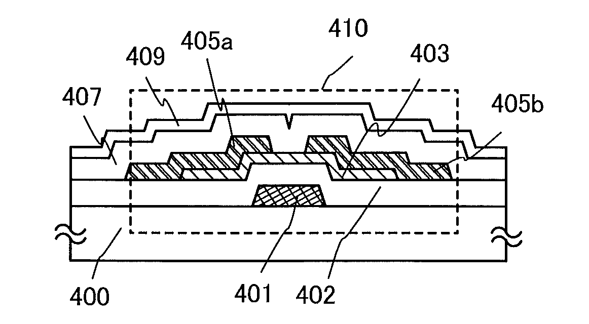
[0037]In this embodiment, an example of a transistor that can be applied to a semiconductor device disclosed in this specification will be described. There is no particular limitation on a structure of the transistor that can be applied to the semiconductor device disclosed in this specification. For example, a staggered transistor, a planar transistor, or the like having a top-gate structure in which a gate electrode is provided above an oxide semiconductor layer with a gate insulating layer interposed therebetween or a bottom-gate structure in which a gate electrode is provided below an oxide semiconductor layer with a gate insulating layer interposed therebetween, can be used. Further, the transistor may have a single gate structure including one channel formation region, a double gate structure including two channel formation regions, or a triple gate structure including three channel formation regions. Alternatively, the transistor may have a dual-gate structure having two gate...

embodiment 2

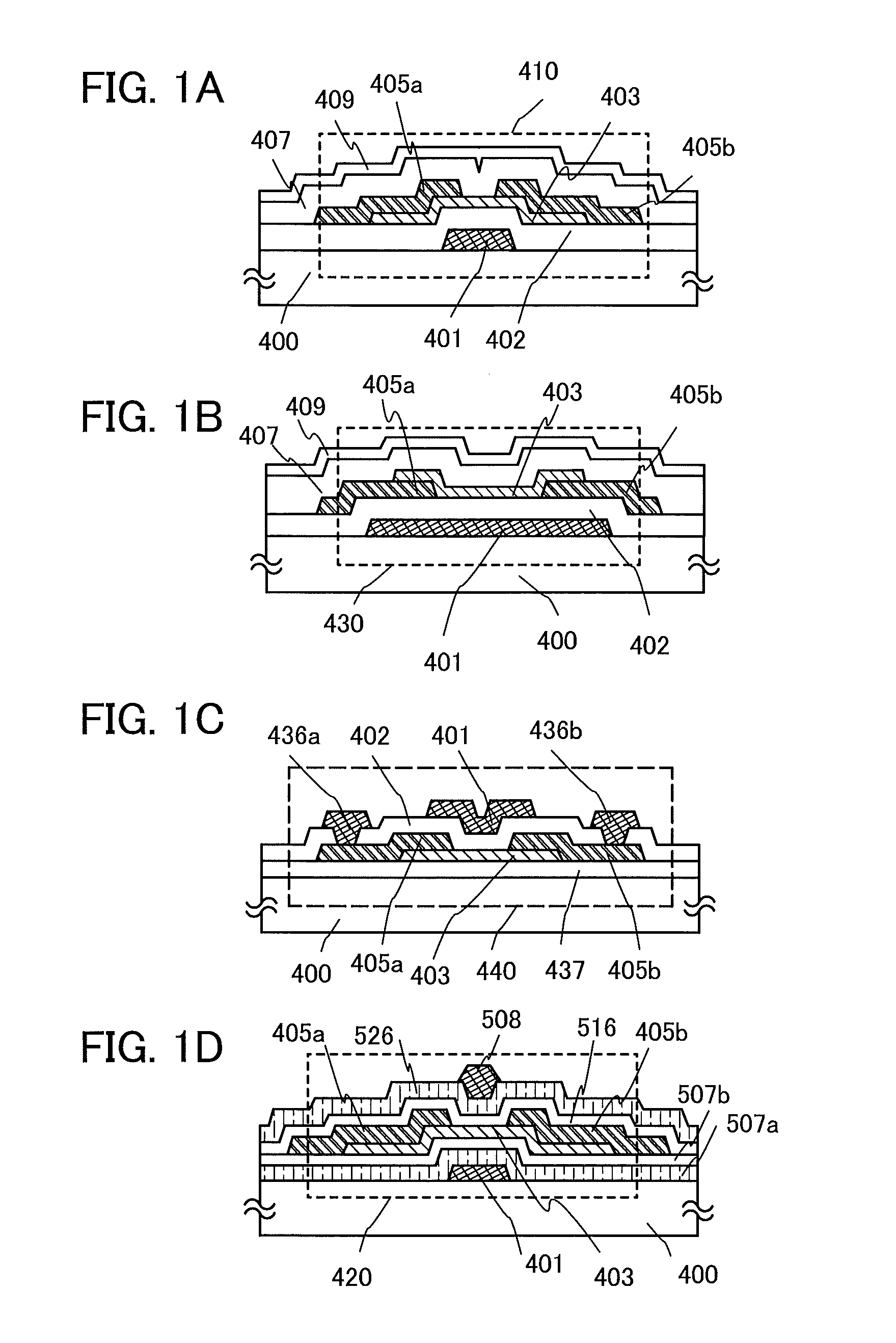
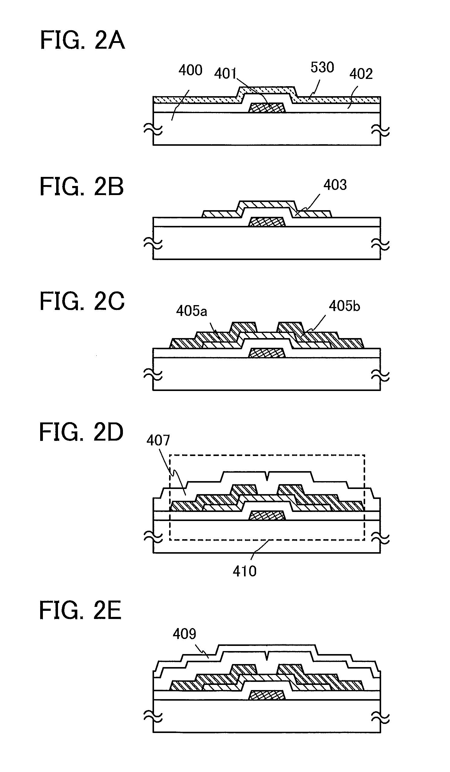
[0093]Next, an example of a manufacturing process of the transistor 440 illustrated in FIG. 1C is described with reference to FIGS. 3A to 3E.

[0094]First, the insulating film 437 is formed over the substrate 400, and an oxide semiconductor film 413 is formed on and in contact with the insulating film 437 (see FIG. 3A).

[0095]The oxide semiconductor film 413 is processed by being etched after a mask having a desired shape is formed over the oxide semiconductor film 413, so that the oxide semiconductor layer can be formed. The mask may be formed by a method such as photolithography or an ink-jet method.

[0096]After that, heat treatment (first heat treatment) is desirably performed on the oxide semiconductor layer. Excessive hydrogen (including water and a hydroxyl group) in the oxide semiconductor layer is removed by the first heat treatment and the structure of the oxide semiconductor layer is modified, so that defect levels in an energy gap can be reduced. The first heat treatment is p...

embodiment 3

[0108]In this embodiment, an example of a manufacturing process part of which is different from that described in Embodiment 2 is described below with reference to FIGS. 4A to 4E. The transistor of this embodiment is different from the transistor of Embodiment 2 in that an insulating film provided under an oxide semiconductor layer has a stacked structure and that the oxide semiconductor layer is formed over a source electrode and a drain electrode.

[0109]First, an insulating film 202 is formed over a substrate 200, and a metal oxide film 204 is formed on and in contact with the insulating film 202 (see FIG. 4A). As the insulating film 202, an inorganic insulating film such as a silicon oxide film, a silicon oxynitride film, an aluminum oxide film, or an aluminum oxynitride film can be typically used. The metal oxide film 204 is formed using a gallium oxide film.

[0110]Next, a conductive film to be a source electrode and a drain electrode (including a wiring formed in the same layer a...


PUM


Abstract

An object is to manufacture a semiconductor device with high reliability by providing the semiconductor device including an oxide semiconductor with stable electric characteristics. In a transistor including an oxide semiconductor layer, a gallium oxide film is used for a gate insulating layer and made in contact with an oxide semiconductor layer. Further, gallium oxide films are provided so as to sandwich the oxide semiconductor layer, whereby reliability is increased. Furthermore, the gate insulating layer may have a stacked structure of a gallium oxide film and a hafnium oxide film.

Description

BACKGROUND OF THE INVENTION[0001]1. Field of the Invention[0002]The present invention relates to a semiconductor device including an oxide semiconductor and a manufacturing method thereof.[0003]In this specification, a semiconductor device generally means a device which can function by utilizing semiconductor characteristics, and an electro-optical device, a semiconductor circuit, and an electronic device are all semiconductor devices.[0004]2. Description of the Related Art[0005]In recent years, a technique for forming a thin film transistor (TFT) by using a thin semiconductor film (having a thickness of approximately several nanometers to several hundred nanometers) formed over a substrate having an insulating surface has attracted attention. Thin film transistors are applied to a wide range of electronic devices such as ICs or electro-optical devices, and prompt development of thin film transistors that are to be used as switching elements in image display devices, in particular, ...

Claims


Application Information

Patent Timeline
Patent Type & Authority Applications(United States)
IPC IPC(8): H01L29/786
CPCH01L29/7869H01L29/42384H01L29/517H01L29/78648H01L29/78696
Inventor YAMAZAKI, SHUNPEI
Owner SEMICON ENERGY LAB CO LTD
Why Eureka
Try Eureka